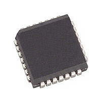
NLXT361PE.A2 S E001 Cortina Systems Inc, NLXT361PE.A2 S E001 Datasheet - Page 24

NLXT361PE.A2 S E001
Manufacturer Part Number
NLXT361PE.A2 S E001
Description
Manufacturer
Cortina Systems Inc
Datasheet
1.NLXT361PE.A2_S_E001.pdf
(55 pages)
Specifications of NLXT361PE.A2 S E001
Number Of Transceivers
1
Operating Supply Voltage (typ)
5V
Screening Level
Industrial
Mounting
Surface Mount
Operating Supply Voltage (min)
4.75V
Operating Supply Voltage (max)
5.25V
Operating Temperature (min)
-40C
Operating Temperature (max)
85C
Lead Free Status / RoHS Status
Not Compliant
LXT361 — Integrated T1/E1 LH/SH Transceiver for DS1/DSX-1 or PRI Applications
3.5.5
3.5.5.1
3.5.5.2
3.6
3.6.1
24
Receive Line Attenuation Indication
The Equalizer Status Register (ESR) provides an approximation of the line attenuation encountered
by the device. The four most significant bits of the register (ESR.LATN7:4) indicate line
attenuation in approximately 2.9 dB steps for both T1 and E1 operation of the receive equalizer.
For instance, if ESR.LATN7:4 is 10 (decimal), then the receiver is seeing a signal attenuated by
approximately 29 dB (2.9 dB x 10) of cable loss.
Built-In Self Test
LXT361 provides a Built-In Self Test (BIST) capability. The BIST exercises the internal circuits by
providing an internal QRSS pattern, running it through the encoders and the transmit drivers then
looping it back through the receive equalizer, jitter attenuator and decoders to the QRSS pattern
detection circuitry. If all the blocks in this data path function correctly, the receive pattern detector
locks onto the pattern. It then pulls INT Low and sets the following bits:
Note that during BIST, the TPOS/TNEG inputs must remain at logic level = 0
The most reliable test will result when a separate TCLK and MCLK are applied and the Line
Build-Out (LBO) is set to -22.5 dB (CR1.EC4:1 = 011x).
Parallel Microprocessor Interface
The LXT361 multiplexed address/data bus and timing/control signals are compatible with both the
Intel and Motorola microprocessors. See
each bus. The LXT361 detects and distinguishes between Intel and Motorola timing and then
automatically selects the appropriate bus timing. The maximum recommended processor speed for
an Intel device is 20 MHz; for a Motorola device, 16.78 MHz. See
page 36
The LXT361 contains five read/write and three read-only registers for control and status purposes.
Table 6 on page 26
function of the register bits.
Interrupt Handling
The LXT361 provides a latched interrupt output pin (INT). When enabled, a change in any of the
Performance Status Register bits will generate an interrupt. An interrupt can also be generated
when the elastic store overflows (TSR.ESOVR) or underflows (TSR.ESUNF). When an interrupt
occurs, the INT output pin is pulled Low. Note that the output stage of the INT pin has internal
pull-down only. Therefore, each device that shares the INT line requires an external pull-up
resistor.
Other Diagnostic Reports
•
•
•
TSR.TQRSS = 1
PSR.QRSS = 1
PSR.BIST = 1
for microprocessor interface timing details.
is a summary of the registers.
Figure 16
Table 7
and
Figure 17
through
Table 15
“Test Specifications” on
for the I/O timing diagram for
identify and explain the
Datasheet


