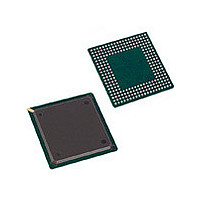
CYP15G0402DXB-BGI Cypress Semiconductor Corp, CYP15G0402DXB-BGI Datasheet - Page 11

CYP15G0402DXB-BGI
Manufacturer Part Number
CYP15G0402DXB-BGI
Description
Manufacturer
Cypress Semiconductor Corp
Datasheet
1.CYP15G0402DXB-BGI.pdf
(29 pages)
Specifications of CYP15G0402DXB-BGI
Lead Free Status / RoHS Status
Not Compliant
Document #: 38-02057 Rev. *G
Pin Descriptions
CYP(V)15G0402DXB HOTLink II SERDES
Operation
The CYP(V)15G0402DXB is a highly configurable device
designed to support reliable transfer of large quantities of data
using high-speed serial links from one or multiple sources to
multiple destinations. This device supports four character-
wide channels.
CYP(V)15G0402DXB Transmit Data Path
Data Path
The transmit path of the CYP(V)15G0402DXB supports four
character-wide data paths. These four data paths are inter-
nally unencoded and require 10-bit input data that may be
pre-encoded or scrambled to achieve sufficient transition
density.
SDASEL
LPENA
LPENB
LPENC
LPEND
LFIA
LFIB
LFIC
LFID
TRSTZ
JTAG Interface
TMS
TCLK
TDO
TDI
Power
V
GND
CC
Name
Three-level Select
static configuration
input
LVTTL Input,
asynchronous,
internal pull-down
LVTTL Output,
Asynchronous
LVCMOS Input,
internal pull-up
LVTTL Input,
internal pull-up
LVTTL Input,
internal pull-down
Three-state
LVTTL Output
LVTTL Input,
internal pull-up
I/O Characteristics Signal Description
CYP(V)15G0402DXB Quad HOTLink II™ SERDES (continued)
[5]
,
Signal Detect Amplitude Level Select. Allows selection of one of three predefined
amplitude trip points for a valid signal indication, as listed in Table 4.
Loop-Back-Enable. Active HIGH. When asserted (HIGH), the transmit serial data from
the associated channel is internally routed to its respective receiver clock and data
recovery (CDR) circuit. The serial output for the channel where LPENx is active is forced
to differential logic “1”, and serial data inputs for that channel are ignored.
Link Fault Indication Output. Active LOW. LFIx is the logical OR of four internal condi-
tions:
Device Reset. Active LOW. Initializes all state machines and counters in the device.
When sampled LOW by the rising edge of REFLCK, this input resets the internal state
machines and sets the Elasticity Buffer pointers to a nominal offset. When the reset is
removed (TRSTZ sampled HIGH by REFCLK↑), the status and data outputs will
become deterministic in fewer than 16 REFCLK cycles.
The BISTLE, OELE, and RXLE latches are reset by TRSTZ.
If the Elasticity Buffer or the Phase Align Buffer are used, TRSTZ should be applied after
power up to initialize the internal pointers into these memory arrays.
Test Mode Select. Used to control access to the JTAG Test Modes. If maintained high
for >5 TCLK cycles, the JTAG test controller is reset. The TAP controller is also reset
automatically upon application of power to the device.
JTAG Test Clock
Test Data Out. JTAG data output buffer which is High-Z while JTAG test mode is not
selected.
Test Data In. JTAG data input port.
+3.3V Power
Signal and Power Ground for all internal circuits.
1. Received serial data frequency outside expected range
2. Analog amplitude below expected levels
3. Transition density lower than expected
4. Receive Channel disabled.
Input Register
The bits in the Input Register for each channel have fixed bit
assignments, as listed in Table 1. Each input register captures
a minimum of 10 bits on each input clock cycle. When parity
checking is enabled, the TXOPx parity input is also captured
in the associated input register.
Input Register Clocking
The transmit Input Registers can be configured to accept data
relative to different clock sources. The selection of the clock
source is controlled by TXCKSEL.
When TXCKSEL = LOW, the Input Registers for all four
transmit channels are clocked by REFCLK↑
TXCKSEL = HIGH, the Input Registers for all four transmit
channels are clocked with TXCLKA↑.
When TXCKSEL is MID, TXCLKx↑ is used as the input
register clock for the associated TXDx[9:0] and TXOPx.
CYP15G0402DXB
CYV15G0402DXB
Page 11 of 29
[4]
. When
[+] Feedback


