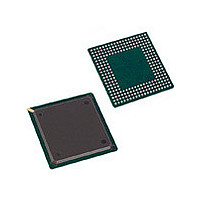
CYP15G0402DXB-BGI Cypress Semiconductor Corp, CYP15G0402DXB-BGI Datasheet - Page 21

CYP15G0402DXB-BGI
Manufacturer Part Number
CYP15G0402DXB-BGI
Description
Manufacturer
Cypress Semiconductor Corp
Datasheet
1.CYP15G0402DXB-BGI.pdf
(29 pages)
Specifications of CYP15G0402DXB-BGI
Lead Free Status / RoHS Status
Not Compliant
Document #: 38-02057 Rev. *G
CYP(V)15G0402DXB DC Electrical Characteristics
Test Loads and Waveforms
Notes:
19. The common mode range defines the allowable range of INPUT+ and INPUT– when INPUT+ = INPUT–. This marks the zero-crossing between the true and
20. Not applicable for AC-coupled interfaces. For AC-coupled interfaces, V
21. Maximum I
22. Typical I
23. Cypress uses constant current (ATE) load configurations and forcing functions. This figure is for reference only. 5-pF differential load reflects tester capacitance,
24. The LVTTL switching threshold is 1.4V. All timing references are made relative to the point where the signal edges crosses the threshold voltage.
V
V
Differential Serial Line Receiver Inputs: INA±, INB±, INC±, IND±
V
V
V
I
I
V
Power Supply
I
I
IHE
ILE
COM
CC
CC
OLC
ODIF
DIFFS
IHE
ILE
Parameter
complement inputs as the signal switches between a logic-1 and a logic-0.
alternating 01 pattern to the associated receive channel.
enabled and sending a continuous alternating 01 pattern to the associated receive channel.
and is recommended at low data rates only.
GND
[19, 20]
V
[17]
th
= 1.4V
≤ 1 ns
CC
CC
is measured under similar conditions except with V
R1 = 590Ω
R2 = 435Ω
C
(Includes fixture and
probe capacitance)
is measured with V
L
Output LOW Voltage
Output Differential Voltage
|(OUT+) – (OUT–)|
Input Differential Voltage |(IN+) – (IN-)|
Highest Input HIGH Voltage
Lowest Input LOW Voltage
Input HIGH Current
Input LOW Current
Common mode input range
Power Supply Current
REFCLK = Max.
Power Supply Current
REFCLK = 125 MHz
(c) LVTTL Input Test Waveform
≤ 7 pF
(a) LVTTL Output Test Load
0.8V
2.0V
CC
Description
3.0V
C
= MAX, parallel outputs unloaded, RX channels enabled, and Serial Line Drivers enabled and sending a continuous
L
2.0V
0.8V
3.3V
R1
R2
Note 23
V
Note 24
≤ 1 ns
th
CC
= 1.4V
= 3.3V, T
100Ω differential load
150Ω differential load
100Ω differential load
150Ω differential load
V
V
DIFFS
Commercial
Industrial
Commercial
Industrial
IN
IN
A
= V
= V
= 25°C, parallel outputs unloaded, RX channels enabled, and Serial Line Drivers
requirement still needs to be satisfied.
Test Conditions
Over the Operating Range (continued)
V
V
IHH
ILL
ILE
IHE
≤ 270 ps
Min.
Max.
20%
(d) CML/LVPECL Input Test Waveform
(b) CML Output Test Load
R
L
= 100Ω
80%
VCC − 1.95
V
V
V
Typ.
CC
CC
CC
–700
V
Min.
V
450
560
100
870
830
IHE
ILE
– 2.0
– 1.1
– 1.1
[22]
CYP15G0402DXB
CYV15G0402DXB
80%
R
L
Note 23
VCC − 0.05
V
V
Max.
CC
CC
Max.
1000
1200
1350
1060
1100
1060
1100
V
900
CC
20%
– 0.7
– 0.7
≤ 270 ps
[21]
Page 21 of 29
Unit
Unit
mV
mV
mV
mA
mA
mA
mA
mA
mA
V
V
V
V
V
[+] Feedback


