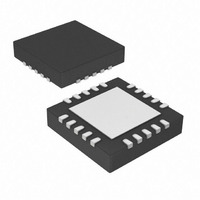
MCP1631-E/ML Microchip Technology, MCP1631-E/ML Datasheet - Page 18

MCP1631-E/ML
Manufacturer Part Number
MCP1631-E/ML
Description
IC,SMPS CONTROLLER,CURRENT-MODE,LLCC,20PIN,PLASTIC
Manufacturer
Microchip Technology
Datasheet
1.MCP1631-EST.pdf
(32 pages)
Specifications of MCP1631-E/ML
Pwm Type
Current Mode
Number Of Outputs
1
Frequency - Max
2MHz
Duty Cycle
10%
Voltage - Supply
3 V ~ 5.5 V
Buck
Yes
Boost
No
Flyback
No
Inverting
No
Doubler
No
Divider
No
Cuk
No
Isolated
Yes
Operating Temperature
-40°C ~ 125°C
Package / Case
20-VQFN Exposed Pad, 20-HVQFN, 20-SQFN, 20-DHVQFN
Frequency-max
2MHz
Output Voltage
3.3 V to 5 V
Output Current
250 mA
Input Voltage
3 V to 5.5 V
Switching Frequency
2 MHz
Operating Temperature Range
- 40 C to + 125 C
Mounting Style
SMD/SMT
Lead Free Status / RoHS Status
Lead free / RoHS Compliant
Lead Free Status / RoHS Status
Lead free / RoHS Compliant
MCP1631/HV/MCP1631V/VHV
5.0
5.1
The MCP1631/MCP1631V can be used to develop
intelligent power management solutions, typical
applications include a multi-chemistry battery charger
used to charge Li-Ion, NiMH or NiCd batteries and
constant current LED drivers.
5.2
The design approach for developing high current
switching battery chargers using the MCP1631 is
described in this section. Depending on input voltage
range, there are two versions of the device that can be
used to accommodate a very wide range of input
voltages.
For a regulated input voltage range of 5V, the
MCP1631/MCP1631V device is used, for this input
voltage application (regulated ac-dc converter or USB
input), the MCP1631/MCP1631V is powered directly
from the 5V dc input.
For input voltages to +16V steady state with +18V
transients, the MCP1631HV/MCP1631VHV, or high
voltage option can be used. The high voltage devices
integrate a low dropout (LDO) linear regulator with a set
output voltage of +3.3V or +5.0V that internally powers
the MCP1631HV/MCP1631VHV and is also capable of
providing 250 mA of bias current for the attached
microcontroller and other circuitry. MCP1631HV/
MCP1631VHV internal power dissipation must be
considered when loading the internal LDO regulator.
For higher input voltages the MCP1631/MCP1631V
can be biased from an external regulated +3.0V to
+5.5V supply.
5.3
The MCP1631/MCP1631V family integrates features
that are necessary to develop programmable current
sources. The SEPIC converter is commonly used in
battery charger applications. The primary or input
inductor is used to filter input current and minimize the
switching noise at the converter input. The primary to
secondary capacitive isolation blocks any dc path from
input to output making the SEPIC safer than Buck or
other non-isolated topologies. The SEPIC rectifier
blocks the reverse path preventing battery leakage, in
other topologies an additional diode for blocking is
necessary
efficiency loss.
The input or primary inductor and output or secondary
inductor are typically constructed from a single
magnetic device with two windings, this is commonly
referred to as a coupled inductor. Using coupled
DS22063A-page 18
APPLICATION INFORMATION
Typical Applications
Battery Charger Design Overview
Programmable Single Ended
Primary Inductive (SEPIC) Current
Source
adding
additional
components
and
inductors has significant advantages in addition to the
size and cost benefits of a single core with multiple
windings.
5.4
For intelligent battery charger design, a microcontroller
is used to generate the proper charge profile, charge
termination, safety timers and battery charger features.
When using the MCP1631/MCP1631V for Li-Ion
battery charger applications, the microcontroller is also
used to generate the constant voltage regulation phase
of the charge cycle. This is accomplished by using the
external reference feature of the MCP1631/MCP1631V
as a programmable current source. The microcontroller
is used to vary the V
MCP1631V. The charge current into the battery is
regulated by the MCP1631/MCP1631V, the level that it
is regulated to is set by the programmability of the
microcontroller.
The internal MCP1631/MCP1631V analog compo-
nents are used to regulate the microcontroller
programmed current. The secondary or battery current
is sensed using amplifier A2, the output of A2 is feed
into the input of the error amplifier A1, the output of A1
sets the peak switch current of the SEPIC converter, it
increases or decreases the battery current to match its
(A1) inputs. By increasing the V
input of A1, the battery current is increased.
5.5
The MCP1631/MCP1631V integrates a high-speed
comparator used to protect the charger and battery
from being exposed to high voltages if the battery is
removed or opens. Comparator C2 is used to sense the
SEPIC output voltage. If the divided down output
voltage becomes higher than the 1.2V internal
MCP1631/MCP1631V reference, the V
output is terminated within 50 ns preventing the build
up of voltage on the SEPIC output.
Peak switch current is limited by the MCP1631/
MCP1631V comparator C1 and error amplifier A1
output voltage clamp. For the MCP1631, the error
amplifier output is clamped at 2.7V. The A1 output is
divided down by 1/3 and compared with CS (current
sense) input. The V
input reaches a level of 1/3 of 2.7V or 0.9V in 12 ns,
preventing the external switch current from becoming
high enough to damage the SEPIC power train.
Internal overtemperature protection limits the device
junction temperature to 150°C preventing catastrophic
failure for overtemperature conditions. Once the
temperature decreases 10°C, the device will resume
normal operation.
Mixed Signal Design
Safety Features
EXT
© 2007 Microchip Technology Inc.
REF
output is turned off if the CS
input of the MCP1631/
REF
or non-inverting
EXT
PWM


