PIC18F25K80-E/MM Microchip Technology, PIC18F25K80-E/MM Datasheet - Page 273
PIC18F25K80-E/MM
Manufacturer Part Number
PIC18F25K80-E/MM
Description
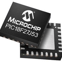
ECAN, 32KB Flash, 4KB RAM, 16 MIPS, 12-bit ADC, CTMU 28 QFN-S 6x6mm TUBE
Manufacturer
Microchip Technology
Series
PIC® XLP™ 18Fr
Datasheet
1.PIC18F25K80-ISO.pdf
(628 pages)
Specifications of PIC18F25K80-E/MM
Core Processor
PIC
Core Size
8-Bit
Speed
64MHz
Connectivity
ECAN, I²C, LIN, SPI, UART/USART
Peripherals
Brown-out Detect/Reset, LVD, POR, PWM, WDT
Number Of I /o
24
Program Memory Size
32KB (16K x 16)
Program Memory Type
FLASH
Eeprom Size
1K x 8
Ram Size
3.6K x 8
Voltage - Supply (vcc/vdd)
1.8 V ~ 5.5 V
Data Converters
A/D 8x12b
Oscillator Type
Internal
Operating Temperature
-40°C ~ 125°C
Package / Case
*
Processor Series
PIC18F25K80
Core
PIC
Data Bus Width
8 bit
Data Ram Size
3648 B
Interface Type
I2C, SPI
Maximum Clock Frequency
64 MHz
Number Of Programmable I/os
24
Number Of Timers
5
Operating Supply Voltage
1.8 V to 5.5 V
Maximum Operating Temperature
+ 125 C
Mounting Style
SMD/SMT
Minimum Operating Temperature
- 40 C
Lead Free Status / RoHS Status
Lead free / RoHS Compliant
Available stocks
Company
Part Number
Manufacturer
Quantity
Price

Part Number:
PIC18F25K80-E/MM
Manufacturer:
MICROCHIP/微芯
Quantity:
20 000


REGISTER 20-2:
In addition to the expanded range of modes available
through the CCP1CON and ECCP1AS registers, the
ECCP module has two additional registers associated
with Enhanced PWM operation and auto-shutdown
features. They are:
• ECCP1DEL – Enhanced PWM Control
• PSTR1CON – Pulse Steering Control
2011 Microchip Technology Inc.
bit 7
Legend:
R = Readable bit
-n = Value at POR
bit 7-5
bit 4
bit 3
bit 2
bit 1
bit 0
U-0
—
Unimplemented: Read as ‘ 0 ’
C5TSEL: CCP5 Timer Selection bit
0 = CCP5 is based off of TMR1/TMR2
1 = CCP5 is based off of TMR3/TMR4
C4TSEL: CCP4 Timer Selection bit
0 = CCP4 is based off of TMR1/TMR2
1 = CCP4 is based off of TMR3/TMR4
C3TSEL: CCP3 Timer Selection bit
0 = CCP3 is based off of TMR1/TMR2
1 = CCP3 is based off of TMR3/TMR4
C2TSEL: CCP2 Timer Selection bit
0 = CCP2 is based off of TMR1/TMR2
1 = CCP2 is based off of TMR3/TMR4
C1TSEL: CCP1 Timer Selection bit
0 = ECCP1 is based off of TMR1/TMR2
1 = ECCP1 is based off of TMR3/TMR4
U-0
—
CCPTMRS: CCP TIMER SELECT REGISTER
W = Writable bit
‘1’ = Bit is set
U-0
—
C5TSEL
R/W-x
Preliminary
U = Unimplemented bit, read as ‘0’
‘0’ = Bit is cleared
PIC18F66K80 FAMILY
C4TSEL
R/W-x
C3TSEL
R/W-x
x = Bit is unknown
C2TSEL
R/W-x
DS39977C-page 273
C1TSEL
R/W-x
bit 0
Related parts for PIC18F25K80-E/MM
Image
Part Number
Description
Manufacturer
Datasheet
Request
R

Part Number:
Description:
Manufacturer:
Microchip Technology Inc.
Datasheet:
Part Number:
Description:
Manufacturer:
Microchip Technology Inc.
Datasheet:
Part Number:
Description:
Manufacturer:
Microchip Technology Inc.
Datasheet:
Part Number:
Description:
Manufacturer:
Microchip Technology Inc.
Datasheet:
Part Number:
Description:
Manufacturer:
Microchip Technology Inc.
Datasheet:
Part Number:
Description:
Manufacturer:
Microchip Technology Inc.
Datasheet:
Part Number:
Description:
Manufacturer:
Microchip Technology Inc.
Datasheet:
Part Number:
Description:
Manufacturer:
Microchip Technology Inc.
Datasheet: