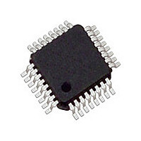
MC33911G5ACR2 Freescale, MC33911G5ACR2 Datasheet - Page 84

MC33911G5ACR2
Manufacturer Part Number
MC33911G5ACR2
Description
Manufacturer
Freescale
Datasheet
1.MC33911G5ACR2.pdf
(92 pages)
Specifications of MC33911G5ACR2
Turn Off Delay Time
10us
Number Of Drivers
2
Operating Temperature (min)
-40C
Operating Temperature (max)
125C
Operating Temperature Classification
Automotive
Lead Free Status / RoHS Status
Compliant
Available stocks
Company
Part Number
Manufacturer
Quantity
Price
Company:
Part Number:
MC33911G5ACR2
Manufacturer:
Freescale Semiconductor
Quantity:
10 000
High Side Control Register - HSCR
Writing to this register returns the High Side Status Register
(HSSR).
PWMHS1 - PWM Input Control Enable.
to control the high side switch. The high side switch must be
enabled (HS1 bit).
HS1 - High Side Switch Control.
High Side Status Register - HSSR
is also returned when writing to the High Side Control
Register (HSCR).
High Side thermal shutdown
setting the HS1OP and HS1CL bits simultaneously.
HS1OP - High Side Switch Open-Load Detection
conducting current below a certain threshold indicating
possible load disconnection.
HS1CL - High Side Current Limitation
operating in current limitation mode.
Table 49. High Side Control Register - $6
Analog Integrated Circuit Device Data
Freescale Semiconductor
Condition
This register controls the operation of the high side driver.
This write-only bit enables/disables the PWMIN input pin
1 = PWMIN input controls HS1 output.
0 = HS1 is controlled only by SPI.
This write-only bit enables/disables the high side switch.
1 = HS1 switch on.
0 = HS1 switch off.
This register returns the status of the high side switch and
A thermal shutdown of the high side drivers is indicated by
This read-only bit signals that the high side switch is
1 = HS1 Open Load detected (or thermal shutdown)
0 = Normal
This read-only bit indicates that the high side switch is
1 = HS1 in current limitation (or thermal shutdown)
0 = Normal
Reset
Reset
Value
Write
Table 50. High Side Status Register - $6/$7
Read
C3
0
0
POR
S3
-
PWMHS1
C2
0
S2
-
POR, Reset mode, ext_reset, HS1
over-temp or (VSOV & HVSE)
HS1OP
C1
0
0
S1
HS1CL
S0
HS1
C0
0
Low Side Control Register - LSCR
Writing the Low Side Control Register (LSCR) will also return
the Low Side Status Register (LSSR).
Table 51. Low Side Control Register - $8
PWMLx - PWM input control enable.
to control the respective low side switch. The corresponding
low side switch must be enabled (LSx bit).
LSx - LSx switch control.
side switch.
Low Side Status Register - LSSR
and is also returned when writing to the LSCR.
Low Side thermal shutdown
setting all LSxOP and LSxCL bits simultaneously.
LSxOP - Low Side Switch Open-Load Detection
conducting current below a certain threshold indicating
possible load disconnection.
LSxCL - Low Side Current Limitation
switch is operating in current limitation mode.
Condition
This register controls the operation of the low side drivers.
This write-only bit enables/disables the PWMIN input pin
1 = PWMIN input controls LSx.
0 = LSx is controlled only by SPI.
This write-only bit enables/disables the corresponding low
1 = LSx switch on.
0 = LSx switch off.
This register returns the status of the low side switches
A thermal shutdown of the low side drivers is indicated by
This read-only bit signals that the low side switches are
1 = LSx Open-load detected (or thermal shutdown)
0 = Normal
This read-only bit indicates that the respective low side
1 = LSx in current limitation (or thermal shutdown)
0 = Normal
Reset
Value
Reset
Write
Table 52. Low Side Status Register - $8/$9
Read
PWMLS2
C3
0
LS2OP
POR
C3
PWMLS1
LOGIC COMMANDS AND REGISTERS
C2
0
FUNCTIONAL DEVICE OPERATIONS
LS2CL
C2
POR, Reset mode, ext_reset, LSx
over-temp or (VSOV & HVSE)
LS2
LS1OP
C1
0
C1
LS1CL
C0
LS1
C0
0
33911
84


