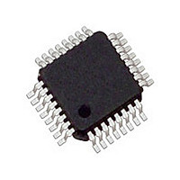
MC34910G5AC Freescale, MC34910G5AC Datasheet - Page 89

MC34910G5AC
Manufacturer Part Number
MC34910G5AC
Description
Manufacturer
Freescale
Datasheet
1.MC34910G5AC.pdf
(90 pages)
Specifications of MC34910G5AC
Turn Off Delay Time
10us
Number Of Drivers
2
Operating Temperature (min)
-40C
Lead Free Status / RoHS Status
Compliant
Available stocks
Company
Part Number
Manufacturer
Quantity
Price
Company:
Part Number:
MC34910G5AC
Manufacturer:
Freescale Semiconductor
Quantity:
10 000
Company:
Part Number:
MC34910G5ACR2
Manufacturer:
Freescale Semiconductor
Quantity:
10 000
89
33910
REVISION HISTORY
1.0
2.0
3.0
4.0
5.0
6.0
7.0
8.0
Revision
Date
5/2007
9/2007
9/2007
2/2008
11/2008
2/2009
3/2009
3/2010
Description of Changes
• Initial Release
• Several textual corrections
• Page 11: “Analog Output offset Ratio” changed to “Analog Output offset” +/-22mV
• Page 11: VSENSE Input Divider Ratio adjusted to 5,0/5,25/5,5
• Page 12: Common mode input impedance corrected to 75k
• Page 13/15: LIN PHYSICAL LAYER parameters adjusted to final LIN specification release
• Revision number incremented at engineering request.
• Changed Functional Block Diagram on page 24.
• Datasheet updated according to the Pass1.2 silicon version electrical parameters
• Add Maximum Rating on I
• Added L1,
• Added
• Minor corrections to
• Updated Freescale form and style
• Added explanation for pins Not Connected (NC).
• Changed VBAT_SHIFT and GND_SHIFT maximum from 10% to 11.5% for both parameters on page 13.
• Combined Complete Data sheet for Part Numbers MC33910BAC and MC34910BAC to the back of this data
• Changed ESD Voltage for Machine Model from ± 200 to ± 150
Sense Gain per characterization at 3 temperatures
Input Divider Ratio (RATIOVSENSE=Vsense/Vadout0) per characterization
Offset per characterization
(LIN),
analog Pin
Dominant / RXD
Over-temperature Shutdown (LIN
1,
sheet.
LIN Control Register -
Serial Data Clock Pin
Temperature Sense Gain
Temperature Sense Analog Output Voltage per characterization
(L1),
Normal Request
Short-circuit:,
ESD
REVISION HISTORY
LINCR, and
Capability,
BUS_NO_GND
(36)
(SCLK),
parameters
Fault Detection Management
section
Mode,
Interrupt),
Master Out Slave In Pin
(18)
RXSHORT - RXD Pin Short-circuit
parameter
,
Sleep
Cyclic Sense ON Time from Stop and Sleep Mode
LIN Receiver Operation
Mode,
(36)
LIN Over-temperature Shutdown / TXD Stuck At
See Figure 16, Temperature Sense
Ω
(MOSI),
Conditions,
Analog Integrated Circuit Device Data
Master In Slave Out Pin
Only,
Lin Physical
(36)
SPI
(36)
, and
,
Protocol,
Internal Chip Temperature
Freescale Semiconductor
VSENSE Output Related
Layer,
L1 - Wake-up input
Gain,
(45)
LIN
(MISO),
,
Lin Bus Pin
Interface,
VSENSE
Digital/


