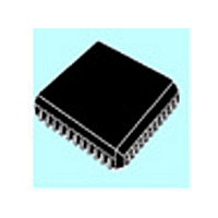
M27C1024-12C6 STMicroelectronics, M27C1024-12C6 Datasheet - Page 4

M27C1024-12C6
Manufacturer Part Number
M27C1024-12C6
Description
Manufacturer
STMicroelectronics
Datasheet
1.M27C1024-12C6.pdf
(16 pages)
Specifications of M27C1024-12C6
Density
1Mb
Organization
64Kx16
Interface Type
Parallel
Bus Type
Parallel
In System Programmable
External
Access Time (max)
100ns
Package Type
PLCC
Reprogramming Technique
OTP
Operating Supply Voltage (typ)
5V
Operating Supply Voltage (min)
4.5V
Operating Supply Voltage (max)
5.5V
Supply Current
50mA
Pin Count
44
Mounting
Surface Mount
Operating Temp Range
-40C to 85C
Operating Temperature Classification
Industrial
Lead Free Status / RoHS Status
Not Compliant
M27C1024
Table 5. AC Measurement Conditions
Figure 5. AC Testing Input Output Waveform
Table 6. Capacitance
Note: 1. Sampled only, not 100% tested.
DEVICE OPERATION
The modes of operations of the M27C1024 are
listed in the Operating Modes table. A single pow-
er supply is required in the read mode. All inputs
are TTL levels except for V
Electronic Signature.
Read Mode
The M27C1024 has two control functions, both of
which must be logically active in order to obtain
data at the outputs. Chip Enable (E) is the power
control and should be used for device selection.
Output Enable (G) is the output control and should
be used to gate data to the output pins, indepen-
4/16
Input Rise and Fall Times
Input Pulse Voltages
Input and Output Timing Ref. Voltages
Symbol
High Speed
Standard
C
C
2.4V
0.4V
OUT
IN
3V
0V
Input Capacitance
Output Capacitance
(1)
(T
Parameter
PP
A
= 25 C, f = 1 MHz)
and 12V on A9 for
1.5V
2.0V
0.8V
AI01822
High Speed
0 to 3V
1.5V
Figure 6. AC Testing Load Circuit
dent of device selection. Assuming that the ad-
dresses are stable, the address access time
(t
(t
of t
has been low and the addresses have been stable
for at least t
Standby Mode
The M27C1024 has a standby mode which reduc-
es the active current from 35mA to 100 A.
The M27C1024 is placed in the standby mode by
applying a TTL high signal to the E input. When in
the standby mode, the outputs are in a high imped-
ance state, independent of the G input.
10ns
Test Conditio n
AVQV
ELQV
V
OE
V
OUT
C L = 30pF for High Speed
C L = 100pF for Standard
C L includes JIG capacitance
IN
DEVICE
UNDER
). Data is available at the output after a delay
) is equal to the delay from E to output
from the falling edge of G, assuming that E
TEST
= 0V
= 0V
AVQV
-t
GLQV
1.3V
Min
.
1N914
3.3k
0.4V to 2.4V
0.8V and 2V
C L
Standard
20ns
Max
12
6
OUT
AI01823B
Unit
pF
pF


