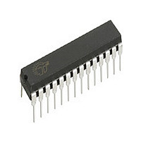
STK11C68P45I Cypress Semiconductor Corp, STK11C68P45I Datasheet - Page 8

STK11C68P45I
Manufacturer Part Number
STK11C68P45I
Description
Manufacturer
Cypress Semiconductor Corp
Type
NVSRAMr
Datasheet
1.STK11C68P45I.pdf
(10 pages)
Specifications of STK11C68P45I
Word Size
8b
Organization
8Kx8
Density
64Kb
Interface Type
Parallel
Access Time (max)
45ns
Operating Supply Voltage (typ)
5V
Package Type
PDIP
Operating Temperature Classification
Industrial
Operating Supply Voltage (max)
5.5V
Operating Supply Voltage (min)
4.5V
Operating Temp Range
-40C to 85C
Pin Count
28
Mounting
Through Hole
Supply Current
65mA
Lead Free Status / RoHS Status
Not Compliant
STK11C68
June 1999
Internally,
the
tile information is transferred into the
After the t
be ready for
RECALL
EEPROM
an unlimited number of times.
POWER-UP RECALL
During power up, or after any low-power condition
(V
latched. When V
voltage of V
be initiated and will take t
If the STK11C68 is in a
power-up
To help avoid this situation, a 10K Ohm resistor
should be connected either between W and system
V
CC
CC
SRAM
or between E and system V
< V
100
80
60
40
20
0
operation in no way alters the data in the
RESET
cells. The nonvolatile data can be recalled
RECALL
RECALL
data is cleared, and second, the nonvola-
RECALL
SWITCH
Figure 2: I
), an internal
READ
cycle time the
, a
CC
50
, the
is a two-step procedure. First,
once again exceeds the sense
RECALL
and
SRAM
CC
Cycle Time (ns)
100
WRITE
RESTORE
(max) Reads
WRITE
RECALL
cycle will automatically
data will be corrupted.
SRAM
150
CC
to complete.
state at the end of
.
TTL
CMOS
operations. The
request will be
will once again
200
SRAM
cells.
4-28
HARDWARE PROTECT
The STK11C68 offers hardware protection against
inadvertent
conditions. When V
operations are inhibited.
LOW AVERAGE ACTIVE POWER
The STK11C68 draws significantly less current
when it is cycled at times longer than 50ns. Figure 2
shows the relationship between I
time. Worst-case current consumption is shown for
both
perature range, V
enable). Figure 3 shows the same relationship for
WRITE
than 100%, only standby current is drawn when the
chip is disabled. The overall average current drawn
by the STK11C68 depends on the following items:
1)
chip enable; 3) the overall cycle rate for accesses;
4) the ratio of
temperature; 6) the V
CMOS
CMOS
100
80
60
40
20
cycles. If the chip enable duty cycle is less
0
vs.
and
Figure 3: I
STORE
TTL
READ
50
TTL
CC
input levels; 2) the duty cycle of
= 5.5V, 100% duty cycle on chip
CC
s to
operation during low-voltage
input levels (commercial tem-
cc
Cycle Time (ns)
CC
100
level; and 7) I/O loading.
< V
WRITE
(max) Writes
SWITCH
150
s; 5) the operating
TTL
, software
CC
CMOS
and
200
READ
STORE
cycle


