LT3494EDDB#PBF Linear Technology, LT3494EDDB#PBF Datasheet
LT3494EDDB#PBF
Specifications of LT3494EDDB#PBF
Available stocks


Related parts for LT3494EDDB#PBF


LT3494EDDB#PBF Summary of contents
Page 1
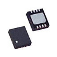
... The LT3494/LT3494A are available in a tiny 8-lead 3mm × 2mm DFN package. , LT, LTC and LTM are registered trademarks of Linear Technology Corporation. All other trademarks are the property of their respective owners. *Patent pending. ...
Page 2
LT3494/LT3494A ABSOLUTE MAXIMUM RATINGS (Note 1) V Voltage ...............................................................16V CC SW Voltage ...............................................................40V CAP Voltage ..............................................................40V V Voltage .............................................................40V OUT SHDN Voltage ...........................................................16V CTRL Voltage ............................................................16V FB Voltage ................................................................2.5V Maximum Junction Temperature .......................... 125°C Operating Temperature Range (Note 2) ... ...
Page 3
ELECTRICAL CHARACTERISTICS temperature range, otherwise specifi cations are at T PARAMETER CTRL Pin Bias Current CTRL to FB Offset Maximum Shunt Current Note 1: Stresses beyond those listed under Absolute Maximum Ratings may cause permanent damage to the device. Exposure ...
Page 4
LT3494/LT3494A TYPICAL PERFORMANCE CHARACTERISTICS Output Voltage vs Temperature 2.0 LT3494 FIGURE 5 CIRCUIT 1.5 1.0 0.5 0 –0.5 –1.0 –1.5 –2.0 –40 – 100 TEMPERATURE (°C) 3494 G04 SHDN Current vs SHDN Voltage 20 15 ...
Page 5
TYPICAL PERFORMANCE CHARACTERISTICS LT3494A Switching Waveforms at No Load FIGURE 6 CIRCUIT V OUT 10mV/DIV AC COUPLED SW VOLTAGE 10V/DIV INDUCTOR CURRENT 50mA/DIV 3494 G13 V = 3.6V 5 s/DIV 16V OUT LT3494 Start-Up Waveforms FIGURE 5 ...
Page 6
LT3494/LT3494A PIN FUNCTIONS SW (Pin 1): Switch Pin. This is the collector of the internal NPN power switch. Minimize the metal trace area connected to this pin to minimize EMI. GND (Pin 2): Ground. Tie directly to local ground plane. ...
Page 7
OPERATION The LT3494/LT3494A use a novel control scheme to pro- vide high effi ciency over a wide range of output current. In addition, this technique keeps the switching frequency above the audio band over all load conditions. The operation of ...
Page 8
LT3494/LT3494A APPLICATIONS INFORMATION Capacitor Selection The small size and low ESR of ceramic capacitors makes them suitable for most LT3494/LT3494A applications. X5R and X7R types are recommended because they retain their capacitance over wider voltage and temperature ranges than other ...
Page 9
APPLICATIONS INFORMATION Connecting the Load to the CAP Node The effi ciency of the converter can be improved by con- necting the load to the CAP pin instead of the V The power loss in the PMOS disconnect circuit is ...
Page 10
LT3494/LT3494A APPLICATIONS INFORMATION the CAP pin will improve effi ciency and lower the stress placed on the internal Schottky diode. Board Layout Considerations As with all switching regulators, careful attention must be paid to the PCB board layout and component ...
Page 11
... SHADED AREA IS ONLY A REFERENCE FOR PIN 1 LOCATION ON THE TOP AND BOTTOM OF PACKAGE Information furnished by Linear Technology Corporation is believed to be accurate and reliable. However, no responsibility is assumed for its use. Linear Technology Corporation makes no representa- tion that the interconnection of its circuits as described herein will not infringe on existing patent rights. ...
Page 12
... I = 4.2A/5.5mA, I OUT(MAX ±34V 40μA, I < 1μA, OUT(MAX 34V 3.2mA, I OUT(MAX 40V 1.2mA, I < 1μA, OUT(MAX ±40V 40μA, I < 1μA, OUT(MAX ±40V 2.5mA, I OUT(MAX 0507 REV B • PRINTED IN USA © LINEAR TECHNOLOGY CORPORATION 2006 < 1μA, SD < 1μA, < 1μA, 3494fb ...