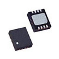
LT3494EDDB#PBF Linear Technology, LT3494EDDB#PBF Datasheet - Page 9

LT3494EDDB#PBF
Manufacturer Part Number
LT3494EDDB#PBF
Description
Manufacturer
Linear Technology
Datasheet
1.LT3494EDDBPBF.pdf
(12 pages)
Specifications of LT3494EDDB#PBF
Operating Temperature (max)
85C
Operating Temperature (min)
-40C
Pin Count
8
Mounting
Surface Mount
Package Type
DFN EP
Case Length
3mm
Screening Level
Industrial
Lead Free Status / RoHS Status
Compliant
Available stocks
Company
Part Number
Manufacturer
Quantity
Price
APPLICATIONS INFORMATION
Connecting the Load to the CAP Node
The effi ciency of the converter can be improved by con-
necting the load to the CAP pin instead of the V
The power loss in the PMOS disconnect circuit is then
made negligible. By connecting the feedback resistor to
the V
feedback resistor string during shutdown since the PMOS
transistor will be open (see Figure 3). The disadvantage
of this method is that the CAP node cannot go to ground
during shutdown, but will be limited to around a diode
drop below V
sink current. Never force external power supplies onto
the CAP or V
(2.2μF to 10μF) should be placed on the node to which
the load is connected.
Maximum Output Load Current
The maximum output current of a particular LT3494/
LT3494A circuit is a function of several circuit variables.
The following method can be helpful in predicting the
maximum load current for a given circuit:
Step 1: Calculate the peak inductor current:
where I
LT3494A respectively. L is the inductance value in Henrys
and V
Step 2: Calculate the inductor ripple current:
where V
I
I
PK
RIPPLE
OUT
IN
=
LIMIT
is the input voltage to the boost circuit.
OUT
I
pin, no quiescent current will be consumed in the
LIMIT
=
is the desired output voltage.
(
CC
OUT
is 0.180A and 0.350A for the LT3494 and
V
3
5
4
+
OUT
. Loads connected to the part should only
Figure 3. Improved Effi ciency
V
SHDN
CTRL
SW
CC
V
pins. The larger value output capacitor
1
IN
LT3494
+
•
1
V
CAP
GND
400 10
–
OUT
FB
8
L
V
IN
L
7
6
2
•
)
•
3494 F03
150 10
–
9
C1
amps
•
–
I
LOAD
9
amps
OUT
pin.
If the inductor ripple current is greater than the peak cur-
rent, then the circuit will only operate in discontinuous
conduction mode. The inductor value should be increased
so that I
to operate only in discontinuous mode, but the output
current capability will be reduced.
Step 3: Calculate the average input current:
Step 4: Calculate the nominal output current:
Step 5: Derate output current:
For low output voltages the output current capability will
be increased. When using output disconnect (load cur-
rent taken from V
the drop in the PMOS switch to be higher resulting in
reduced output current capability than those predicted
by the preceding equations.
Inrush Current
When V
age while the output capacitor is discharged, a higher
level of inrush current may fl ow through the inductor
and integrated Schottky diode into the output capacitor.
Conditions that increase inrush current include a larger
more abrupt voltage step at V
tied to the CAP pin and an inductor with a low saturation
current. While the internal diode is designed to handle
such events, the inrush current should not be allowed to
exceed 1A. For circuits that use output capacitor values
within the recommended range and have input voltages
of less than 5V, inrush current remains low, posing no
hazard to the device. In cases where there are large steps
at V
at the CAP pin, inrush current should be measured to
ensure safe operation. The LT3494A circuits experience
higher levels of current during start-up and steady-state
operation. An external diode placed from the SW pin to
I
I
I
OUT
IN AVG
OUT NOM
CC
(
(
(more than 5V) and/or a large capacitor is used
= I
RIPPLE
CC
)
OUT(NOM)
is stepped from ground to the operating volt-
=
)
I
=
PK
< I
I
IN AVG
PK
–
(
OUT
I
. An application circuit can be designed
RIPPLE
• 0.7 amps
2
), these higher currents will cause
)
V
•
OUT
LT3494/LT3494A
V
IN
amps
• .
IN
0 75
, a larger output capacitor
amps
3494fb
9


