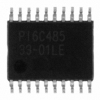
PI6C48533-01LE Pericom Semiconductor, PI6C48533-01LE Datasheet

PI6C48533-01LE
Specifications of PI6C48533-01LE
Related parts for PI6C48533-01LE
PI6C48533-01LE Summary of contents
Page 1
... CLK_SEL 09-0110 Differential/LVCMOS to LVPECL Fanout Buffer Description The PI6C48533- high-performance low-skew LVPECL fanout buffer. PI6C48533-01 features two selectable differential inputs and translates to four LVPECL ultra-low jitter outputs. The inputs can also be confi gured to single-ended with external resistor bias circuit. The CLK input accepts LPECL or LVDS or LVHSTL or SSTL or HCSL signals, and PCLK input accepts LVPECL or SSTL or CML signals ...
Page 2
... LVCMOS/LVTTL level with 50KΩ pull-up Conditions (1) Selected Source CLK, CLK Diasbled: Low n PCLK, PCLK Disabled: Low n CLK, CLK Enabled n PCLK, PCLK Enabled n 2 3.3V Low Skew 1-to-4 Min. Typ. Max Outputs Diasbled: High Disabled: High Enabled Enabled PI6C48533-01 x Units pF KΩ PS8737B 12/15/09 ...
Page 3
... Single Ended to Differential Conditions Referenced to GND Referenced to GND Referenced to GND 3 3.3V Low Skew 1-to-4 Input to Output Mode None Inverting None Inverting None Inverting None Inverting Inverting Inverting Min. Typ. Max. 4.6 -0.5 V +0.5V CC -0.5 V +0.5V CC -65 150 PI6C48533-01 Polarity Units PS8737B 12/15/09 ...
Page 4
... Low Skew 1-to-4 Min. Typ. Max. 3.0 3.3 3.6 - 3.0V to 3.6V unless otherwise stated.) Min. Typ. Max -0.3 0.8 150 5 -5 -150 Min. Typ. Max. 5 150 = 0V -150 = 0V -5 0.15 1 +0.5 EE 0.85V +0.3V CC PI6C48533-01 Units Units +0 μA Units μ PS8737B 12/15/09 ...
Page 5
... Conditions (3) 20% - 80% 5 3.3V Low Skew 1-to-4 Min. Typ. Max. 5 150 = 0V -150 0.6 1.0 +0.3V 2V, unless otherwise stated below. CC Min. Typ. Max. 500 800 1.0 2.0 100 150 75 300 40 60 PI6C48533-01 Units μA -0.9 V -1.6 ) Units MHz PS8737B 12/15/09 ...
Page 6
... R2 might need to be adjusted to postion the V_REF in the center of the input voltage swing. For example, if the input clock swing is only 2.5V and V = 3.3V, V_REF should be 1.25V and R1/R2 = 0.609. CC Figure 2: Single-ended Signal Driving Differential Input 09-0110 Differential/LVCMOS to LVPECL Fanout Buffer V R1 Single Ended 1K Clock Input C1 R2 0.1μ 3.3V Low Skew 1-to-4 CC CLK nCLK PI6C48533- gener- CC PS8737B 12/15/09 ...
Page 7
... Ref: JEDEC MO-153F/AC Note: • For latest package info, please check: http://www.pericom.com/products/packaging/mechanicals.php (1,2) Ordering Information Ordering Code PI6C48533-01LE Notes: 1. Thermal characteristics can be found on the company web site at www.pericom.com/packaging Pb-free and Green Pericom Semiconductor Corporation • 1-800-435-2336 • www.pericom.com 09-0110 Differential/LVCMOS to LVPECL Fanout Buffer 4 ...


