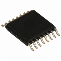
CY2DL814ZXC Cypress Semiconductor Corp, CY2DL814ZXC Datasheet

CY2DL814ZXC
Specifications of CY2DL814ZXC
Available stocks
Related parts for CY2DL814ZXC
CY2DL814ZXC Summary of contents
Page 1
... IN+ IN- LVDS / LVPECL / LVTTL CONFIG CNTRL Cypress Semiconductor Corporation Document #: 38-07057 Rev. *B 1:4 Clock Fanout Buffer Description The Cypress CY2 series of network circuits is produced using advanced 0.35-micron CMOS technology, achieving the industry’s fastest logic. The Cypress CY2DL814 fanout buffer features a single LVDS-, LVPECL-, or LVTTL-compatible input and four LVDS output pairs ...
Page 2
Pin Description Pin Number Pin Name 6,7 IN+, IN– 3 CNTRL 2 CONFIG 1,8 EN1, EN2 16,15,14,13 Q1A, Q1B, Q2A, 12,11,10,9 Q2B, Q3A, Q3B, Q4A, Q4B [1, 2] Maximum Ratings Storage Temperature: ................................ –65°C ...
Page 3
Table 3. Input Receiver Configuration for Differential or LVTTL/LVCMOS CONFIG Pin 2 Binary Value Input Receiver Family 1 LVTTL in LVCMOS 0 LVDS LVPECL Table 4. Function Control of the TTL Input Logic Used to Accept or Invert the Input ...
Page 4
Table 8. D.C Electrical Characteristics: 3.3V–LVTTL/LVCMOS Input Parameter Description V Input High Voltage IH V Input Low Voltage IL I Input High Current IH I Input Low Current IL I Input High Current I V Clamp Diode Voltage IK V ...
Page 5
Table 12.High Frequency Parametrics Parameter Description Fmax Maximum frequency V = 3.3V DD Fmax(20) Maximum frequency Minimum pulse Pulse Generator B V1A 1 V1B V0Y V0Z Figure 1. ...
Page 6
... Lead-free CY2DL814ZXI CY2DL814ZXIT CY2DL814SXI CY2DL814SXIT CY2DL814ZXC CY2DL814ZXCT CY2DL814SXC CY2DL814SXCT Notes: 7. LVCMOS/LVTTL single ended input value. Ground either input: when on the B side then non-inversion takes place side is grounded, the signal becomes the complement of the input on B side. See Table 4. 8. LVPECL or LVDS differential input value. ...
Page 7
... Document #: 38-07057 Rev. *B © Cypress Semiconductor Corporation, 2005. The information contained herein is subject to change without notice. Cypress Semiconductor Corporation assumes no responsibility for the use of any circuitry other than circuitry embodied in a Cypress product. Nor does it convey or imply any license under patent or other rights. Cypress products are not warranted nor intended to be used for medical, life support, life saving, critical control or safety applications, unless pursuant to an express written agreement with Cypress ...
Page 8
Document Title: ComLink™ Series CY2DL814 1:4 Clock Fanout Buffer Document Number: 38-07057 Issue REV. ECN NO. Date ** 115362 07/10/02 *A 122744 12/14/02 *B 384077 See ECN Document #: 38-07057 Rev. *B Orig. of Change Description of Change EHX New ...


