CY2DL814ZXC Cypress Semiconductor Corp, CY2DL814ZXC Datasheet - Page 2
CY2DL814ZXC
Manufacturer Part Number
CY2DL814ZXC
Description
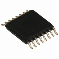
IC CLK FANOUT BUFFER 1:4 16TSSOP
Manufacturer
Cypress Semiconductor Corp
Series
ComLink™r
Type
Fanout Buffer (Distribution)r
Datasheet
1.CY2DL814ZXI.pdf
(8 pages)
Specifications of CY2DL814ZXC
Package / Case
16-TSSOP
Number Of Circuits
1
Ratio - Input:output
1:4
Differential - Input:output
Yes/Yes
Input
LVDS, LVPECL, LVTTL
Output
LVDS
Frequency - Max
400MHz
Voltage - Supply
3.135 V ~ 3.465 V
Operating Temperature
0°C ~ 70°C
Mounting Type
Surface Mount
Frequency-max
400MHz
Number Of Outputs
8
Max Input Freq
400 MHz
Propagation Delay (max)
4 ns
Supply Voltage (max)
3.465 V
Supply Voltage (min)
3.135 V
Maximum Power Dissipation
750 mW
Maximum Operating Temperature
+ 70 C
Minimum Operating Temperature
0 C
Mounting Style
SMD/SMT
Lead Free Status / RoHS Status
Lead free / RoHS Compliant
Available stocks
Company
Part Number
Manufacturer
Quantity
Price
Company:

Part Number:
CY2DL814ZXC
Manufacturer:
SOLIDLITE
Quantity:
8 623


Document #: 38-07057 Rev. *B
Pin Description
Maximum Ratings
Storage Temperature: ................................ –65°C to + 150°C
Ambient Temperature:................................... –40°C to +85°C
Supply Voltage to Ground Potential
(Inputs and V
Supply Voltage to Ground Potential
Table 1. EN1 EN2 Function Table–Differential Input Mode
Table 2. Output Drive Control for Standard and Bus/B/High Drive B
Notes:
1. Stresses greater than those listed under absolute maximum ratings may cause permanent damage to the device. This is intended to be a stress rating only and
2. Multiple Supplies: The voltage on any input or I/O pin cannot exceed the power pin during power-up. Power supply sequencing is NOT required.
CNTRL Pin 3 Binary Value
Pin Number
functional operation of the device at these or any other conditions above those indicated in the operation sections of this specification is not implied. Exposure to
absolute maximum rating conditions for extended periods may affect reliability.
16,15,14,13
12,11,10,9
6,7
1,8
EN1
3
2
4
5
H
H
X
X
L
CC
Enable Logic
0
1
only)....................................... –0.3V to 4.6V
Q1A, Q1B, Q2A,
Q3A, Q3B, Q4A,
Pin Name
[1, 2]
EN1, EN2
CONFIG
IN+, IN–
CNTRL
Q2B,
Q4B
V
G
DD
ND
EN2
H
X
X
L
L
High Drive/Bus/B
Pin Standard Interface
Drive STD
Standard
LVTTL/LVCMOS
LVTTL/LVCMOS
LVTTL/LVCMOS
Configurable
POWER
POWER
LDVS
IN+
H
H
X
L
L
Input
(Outputs only) ........................................ –0.3V to V
DC Input Voltage ................................... –0.3V to V
DC Output Voltage................................. –0.3V to V
Power Dissipation........................................................ 0.75W
Differential input pair or single line.
Converts into a High drive driver from a standard LVDS.
Standard drive (logic = 0)
B/High drive/Bus (logic = 1)
Converts inputs (IN
Enable/disable logic. See Table 1 below for details.
Differential outputs.
Positive supply voltage
Ground
LVPECL default. See config below.
LVPECL/LVDS (logic = 0)
To LVTTL/LVCMOS (logic = 1)
IN–
H
H
X
L
L
Impedance
100 ohm
100 ohm
50 ohm
50 ohm
+
/IN
Description
–
), (EN, EN#) from the default
QnA
H
H
Z
L
L
ComLink™ Series
V0 = Voutput
V = 1/2 * V0
V = 2 * V0
V = V0
Output Voltage Value
Outputs
CY2DL814
QnB
Page 2 of 8
H
H
Z
L
L
DD
DD
DD
+ 0.3V
+ 0.3V
+ 0.9V
Related parts for CY2DL814ZXC
Image
Part Number
Description
Manufacturer
Datasheet
Request
R

Part Number:
Description:
Manufacturer:
Cypress Semiconductor Corp
Datasheet:
Part Number:
Description:
Manufacturer:
Cypress Semiconductor Corp
Datasheet:
Part Number:
Description:
Manufacturer:
Cypress Semiconductor Corp
Datasheet:
Part Number:
Description:
Manufacturer:
Cypress Semiconductor Corp
Datasheet:
Part Number:
Description:
Manufacturer:
Cypress Semiconductor Corp
Datasheet: