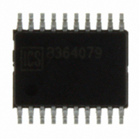
ICS85356AGILF IDT, Integrated Device Technology Inc, ICS85356AGILF Datasheet - Page 8

ICS85356AGILF
Manufacturer Part Number
ICS85356AGILF
Description
IC CLK MUX 2:1 DIFF HS 20-TSSOP
Manufacturer
IDT, Integrated Device Technology Inc
Series
HiPerClockS™r
Type
Multiplexerr
Datasheet
1.ICS85356AGILF.pdf
(15 pages)
Specifications of ICS85356AGILF
Number Of Circuits
2
Ratio - Input:output
2:1
Differential - Input:output
Yes/Yes
Input
HCSL, LVDS, LVHSTL, LVPECL, SSTL
Output
LVPECL
Frequency - Max
900MHz
Voltage - Supply
3 V ~ 3.6 V
Operating Temperature
-40°C ~ 85°C
Mounting Type
Surface Mount
Package / Case
20-TSSOP
Frequency-max
900MHz
Number Of Clock Inputs
4/2
Mode Of Operation
Differential
Output Frequency
900MHz
Output Logic Level
ECL/LVPECL
Operating Supply Voltage (min)
-3/3V
Operating Supply Voltage (typ)
-3.3/3.3V
Operating Supply Voltage (max)
-3.8/3.6V
Package Type
TSSOP
Operating Temp Range
-40C to 85C
Operating Temperature Classification
Industrial
Mounting
Surface Mount
Pin Count
20
Lead Free Status / RoHS Status
Lead free / RoHS Compliant
Other names
800-1175
800-1175-5
800-1175
85356AGILF
800-1175-5
800-1175
85356AGILF
ICS85356I Data Sheet
Termination for 3.3V LVPECL Outputs
The clock layout topology shown below is a typical termination for
LVPECL outputs. The two different layouts mentioned are
recommended only as guidelines.
The differential outputs are low impedance follower outputs that
generate ECL/LVPECL compatible outputs. Therefore, terminating
resistors (DC current path to ground) or current sources must be
used for functionality. These outputs are designed to drive 50Ω
Figure 3A. 3.3V LVPECL Output Termination
ICS85356AMI REVISION B MAY 10, 2010
RTT =
((V
3.3V
OH
LVPECL
+ V
OL
) / (V
1
CC
Z
Z
– 2)) – 2
o
o
= 50Ω
= 50Ω
* Z
R1
50Ω
o
RTT
R2
50Ω
V
+
_
CC
3.3V
- 2V
Input
8
transmission lines. Matched impedance techniques should be used
to maximize operating frequency and minimize signal distortion.
Figures 3A and 3B show two different layouts which are
recommended only as guidelines. Other suitable clock layouts may
exist and it would be recommended that the board designers
simulate to guarantee compatibility across all printed circuit and clock
component process variations.
Figure 3B. 3.3V LVPECL Output Termination
3.3V
2:1, DIFFERENTIAL-TO-3.3V LVPECL/ECL CLOCK MULTIPLEXER
LVPECL
Z
Z
o
o
= 50Ω
= 50Ω
R3
125Ω
©2010 Integrated Device Technology, Inc.
R1
84Ω
3.3V
R4
125Ω
R2
84Ω
+
_
3.3V
Input


