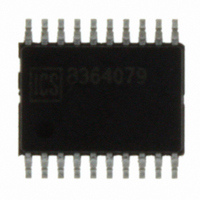
ICS85356AGILF IDT, Integrated Device Technology Inc, ICS85356AGILF Datasheet - Page 9

ICS85356AGILF
Manufacturer Part Number
ICS85356AGILF
Description
IC CLK MUX 2:1 DIFF HS 20-TSSOP
Manufacturer
IDT, Integrated Device Technology Inc
Series
HiPerClockS™r
Type
Multiplexerr
Datasheet
1.ICS85356AGILF.pdf
(15 pages)
Specifications of ICS85356AGILF
Number Of Circuits
2
Ratio - Input:output
2:1
Differential - Input:output
Yes/Yes
Input
HCSL, LVDS, LVHSTL, LVPECL, SSTL
Output
LVPECL
Frequency - Max
900MHz
Voltage - Supply
3 V ~ 3.6 V
Operating Temperature
-40°C ~ 85°C
Mounting Type
Surface Mount
Package / Case
20-TSSOP
Frequency-max
900MHz
Number Of Clock Inputs
4/2
Mode Of Operation
Differential
Output Frequency
900MHz
Output Logic Level
ECL/LVPECL
Operating Supply Voltage (min)
-3/3V
Operating Supply Voltage (typ)
-3.3/3.3V
Operating Supply Voltage (max)
-3.8/3.6V
Package Type
TSSOP
Operating Temp Range
-40C to 85C
Operating Temperature Classification
Industrial
Mounting
Surface Mount
Pin Count
20
Lead Free Status / RoHS Status
Lead free / RoHS Compliant
Other names
800-1175
800-1175-5
800-1175
85356AGILF
800-1175-5
800-1175
85356AGILF
ICS85356I Data Sheet
Power Considerations
This section provides information on power dissipation and junction temperature for the ICS85356I.
Equations and example calculations are also provided.
1.
The total power dissipation for the ICS85356I is the sum of the core power plus the power dissipated in the load(s).
The following is the power dissipation for V
NOTE: Please refer to Section 3 for details on calculating power dissipated in the load.
Total Power_
2. Junction Temperature.
Junction temperature, Tj, is the temperature at the junction of the bond wire and bond pad directly affects the reliability of the device. The
maximum recommended junction temperature is 125°C. Limiting the internal transistor junction temperature, Tj, to 125°C ensures that the bond
wire and bond pad temperature remains below 125°C.
In order to calculate junction temperature, the appropriate junction-to-ambient thermal resistance θ
a multi-layer board, the appropriate value is 83.2°C/W per Table 6B below.
Therefore, Tj for an ambient temperature of 85°C with all outputs switching is:
This calculation is only an example. Tj will obviously vary depending on the number of loaded outputs, supply voltage, air flow and the type of
board (single layer or multi-layer).
Table 6A. Thermal Resistance
NOTE: Most modern PCB design use multi-layered boards. The data in the second row pertains to most designs.
Table 6B. Thermal Resistance
NOTE: Most modern PCB design use multi-layered boards. The data in the second row pertains to most designs.
ICS85356AMI REVISION B MAY 10, 2010
Linear Feet per Minute
Single-Layer PCB, JEDEC Standard Test Boards
Multi-Layer PCB, JEDEC Standard Test Boards
Linear Feet per Minute
Single-Layer PCB, JEDEC Standard Test Boards
Multi-Layer PCB, JEDEC Standard Test Boards
Power Dissipation.
•
•
Power (core)
Power (outputs)
If all outputs are loaded, the total power is 2 * 30mW = 60mW
The equation for Tj is as follows: Tj = θ
Tj = Junction Temperature
θ
Pd_total = Total Device Power Dissipation (example calculation is in section 1 above)
T
85°C + 0.204W * 73.2°C/W = 99.9°C. This is well below the limit of 125°C.
JA
A
= Ambient Temperature
= Junction-to-Ambient Thermal Resistance
MAX
(3.6V, with all outputs switching) = 144mW + 60mW = 204mW
MAX
MAX
= V
= 30mW/Loaded Output pair
CC_MAX
θ
θ
JA
JA
* I
EE_MAX
for 20 Lead SOIC, Forced Convection
for 20 Lead TSSOP, Forced Convection
CC
= 3.3V + 0.3V = 3.6V, which gives worst case results.
JA
= 3.6V * 40mA = 144mW
* Pd_total + T
θ
θ
JA
JA
A
114.5°C/W
73.2°C/W
83.2°C/W
46.2°C/W
by Velocity
by Velocity
0
0
9
2:1, DIFFERENTIAL-TO-3.3V LVPECL/ECL CLOCK MULTIPLEXER
98.0°C/W
66.6°C/W
65.7°C/W
39.7°C/W
200
200
JA
must be used. Assuming no air flow and
©2010 Integrated Device Technology, Inc.
88.0°C/W
63.5°C/W
57.5°C/W
36.8°C/W
500
500


