NB6HQ14MMNHTBG ON Semiconductor, NB6HQ14MMNHTBG Datasheet
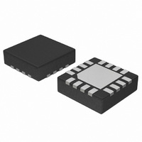
IC BUFFER FANOUT 1:4 CML 16-QFN

NB6HQ14MMNHTBG

Manufacturer Part Number
NB6HQ14MMNHTBG
Description
IC BUFFER FANOUT 1:4 CML 16-QFN
Manufacturer
ON Semiconductor
Series
ECLinPS MAX™r
Type
Fanout Buffer (Distribution), Multiplexerr
Datasheet

Specifications of NB6HQ14MMNHTBG

Number Of Circuits
1
Ratio - Input:output
1:4
Differential - Input:output
Yes/Yes
Input
CML, LVDS, LVPECL
Output
CML
Frequency - Max
5GHz
Voltage - Supply
2.375 V ~ 2.625 V
Operating Temperature
-40°C ~ 85°C
Mounting Type
Surface Mount
Package / Case
16-TFQFN Exposed Pad
Frequency-max
5GHz
Logic Family
NB6HQ14
Logic Type
CML Fanout Buffer
Supply Voltage (max)
2.625 V
Supply Voltage (min)
2.375 V
Maximum Operating Temperature
+ 85 C
Mounting Style
SMD/SMT
Data Rate
10 Gbps
Minimum Operating Temperature
- 40 C
Output Current
+/- 40 mA
Output Voltage
- 0.5 to + 3.5 V
Propagation Delay Time
220 ps
Supply Current
75 mA
Lead Free Status / RoHS Status
Lead free / RoHS Compliant

Available stocks

Company
Part Number
Manufacturer
Quantity
Price
Part Number:
NB6HQ14MMNHTBG
Manufacturer:
ON
Quantity:
5
Part Number:
NB6HQ14MMNHTBG
Manufacturer:
ON Semiconductor
Quantity:
65
NB6HQ14M
2.5V 5GHz / 6.5Gbps
Differential Input to 1.8V /
2.5V 1:4 CML Clock / Data
Fanout Buffer
Input Equalizer
Multi−Level Inputs w/ Internal Termination
Description
buffer with a selectable Equalizer receiver. When placed in series with
a Clock /Data path operating up to 5 GHz or 6.5 Gb/s, respectively, the
NB6HQ14M inputs will compensate the degraded signal transmitted
across a FR4 PCB backplane or cable interconnect and output four
identical CML copies of the input signal. Therefore, the serial data rate
is increased by reducing Inter−Symbol Interference (ISI) caused by
losses in copper interconnect or long cables. The EQualizer ENable
pin (EQEN) allows the IN/IN inputs to either flow through or bypass
the Equalizer section. Control of the Equalizer function is realized by
setting EQEN; When EQEN is set Low, the IN/IN inputs bypass the
Equalizer. When EQEN is set High, the IN/IN inputs flow through the
Equalizer. The default state at start−up is LOW. As such, NB6HQ14M
is ideal for SONET, GigE, Fiber Channel, Backplane and other
Clock/Data distribution applications.
resistors that are accessed through the VT pin. This feature allows the
NB6HQ14M to accept various logic level standards, such as LVPECL,
CML or LVDS. The outputs have the flexibility of being powered by
either a 2.5 V or 1.8 V supply. The 1:4 fanout design was optimized
for low output skew applications.
high performance clock products.
Features
© Semiconductor Components Industries, LLC, 2009
June, 2009 − Rev. 0
The NB6HQ14M is a high performance differential 1:4 CML fanout
The differential inputs incorporate internal 50 W termination
The NB6HQ14M is a member of the ECLinPS MAX™ family of
2.625 V
Input Data Rate > 6.5 Gb/s
Input Clock Frequency > 5 GHz
170 ps Typical Propagation Delay
35 ps Typical Rise and Fall Times
< 15 ps Output Skew
< 0.8 ps RMS Clock Jitter
< 10 ps pp of Data Dependent Jitter
Differential CML Outputs, 400 mV Peak−to−Peak, Typical
Selectable Input Equalization
Operating Range: V
−40°C to +85°C Ambient Operating Temperature
These are Pb−Free Devices
Internal Input Termination Resistors, 50 W
CC
= 2.375 V to 2.625 V, V
w/ Selectable
CCO
= 1.71 V to
1
See detailed ordering and shipping information in the package
dimensions section on page 10 of this data sheet.
*For additional marking information, refer to
MN SUFFIX
CASE 485G
(Note: Microdot may be in either location)
Application Note AND8002/D.
QFN−16
SIMPLIFIED BLOCK DIAGRAM
1
ORDERING INFORMATION
A
L
Y
W
G
http://onsemi.com
= Assembly Location
= Wafer Lot
= Year
= Work Week
= Pb−Free Package
EQ
Publication Order Number:
1
16
DIAGRAM*
MARKING
ALYWG
Q14M
NB6H
G
NB6HQ14M/D

Related parts for NB6HQ14MMNHTBG

NB6HQ14MMNHTBG Summary of contents

Page 1

NB6HQ14M 2.5V 5GHz / 6.5Gbps Differential Input to 1.8V / 2.5V 1:4 CML Clock / Data Fanout Buffer w/ Selectable Input Equalizer Multi−Level Inputs w/ Internal Termination Description The NB6HQ14M is a high performance differential 1:4 CML fanout buffer with ...

Page 2

Multi−Level Inputs LVPECL, LVDS, CML VREFAC V CC GND EQEN (Equalizer Enable Figure 1. 0 2:1 MUX EQ 1 Detailed Block Diagram of NB6HQ14M http://onsemi.com 2 CML Outputs V CC0 Q0 ...

Page 3

GND NB6HQ14M VREFAC EQEN CCO Figure 2. QFN−16 Pinout (Top View) Table 2. PIN DESCRIPTION Pin Name I/O ...

Page 4

Table 3. ATTRIBUTES ESD Protection R − EQEN Input Pulldown Resistor PD Moisture Sensitivity (Note 3) Flammability Rating Transistor Count Meets or exceeds JEDEC Spec EIA/JESD78 IC Latchup Test 3. For additional information, see Application Note AND8003/D. Table 4. MAXIMUM ...

Page 5

Table 5. DC CHARACTERISTICS, MULTI−LEVEL INPUTS T = −40°C to 85°C (Note 5) A Symbol Characteristic POWER SUPPLY / CURRENT V Power Supply Voltage CC V CCO I Power Supply Current for VCC (Inputs and Outputs Open Power ...

Page 6

Table 6. AC CHARACTERISTICS V Symbol f Maximum Input Clock Frequency; MAX f Maximum Operating Data Rate (PRBS23) DATAMAX V Output Voltage Amplitude, EQEN = (Note 15) OUTPP (See Figures 3 and 10 Propagation Delay, ...

Page 7

Figure 6. Differential Input Driven Single−Ended IHmax V thmax V ILmax thmin V IHmin V ILmin GND ...

Page 8

Driver Q Q DJ1 Figure 12. Typical NB6HQ14M Equalizer Application and Interconnect with PRBS23 pattern at 6.5 Gbps, EQEN = FR4 − 12 Inch Backplane IN IN DJ2 http://onsemi.com 8 NB6HQ14M EQualizer EQEN = 1 DJ3 ...

Page 9

LVPECL − Driver GND/V EE Figure 13. LVPECL Interface CML V ...

Page 10

... W ORDERING INFORMATION Device NB6HQ14MMNG NB6HQ14MMNHTBG NB6HQ14MMNTXG †For information on tape and reel specifications, including part orientation and tape sizes, please refer to our Tape and Reel Packaging Specifications Brochure, BRD8011/D. NB6HQ14M Receiver V V (Receiver CCO CC CCO V (Receiver GND Figure 18. Typical CML Output Structure ...

Page 11

... E2 e 3.25 0.128 *For additional information on our Pb−Free strategy and soldering details, please download the ON Semiconductor Soldering and Mounting Techniques Reference Manual, SOLDERRM/D. N. American Technical Support: 800−282−9855 Toll Free USA/Canada Europe, Middle East and Africa Technical Support: Phone: 421 33 790 2910 Japan Customer Focus Center Phone: 81− ...

Related keywords