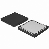
NB100LVEP221MNG ON Semiconductor, NB100LVEP221MNG Datasheet - Page 7

NB100LVEP221MNG
Manufacturer Part Number
NB100LVEP221MNG
Description
IC CLK DVR 1:20 DIFF 52-QFN
Manufacturer
ON Semiconductor
Series
100LVEPr
Type
Fanout Buffer (Distribution), Multiplexerr
Datasheet
1.NB100LVEP221MNRG.pdf
(12 pages)
Specifications of NB100LVEP221MNG
Number Of Circuits
1
Ratio - Input:output
2:20
Differential - Input:output
Yes/Yes
Input
ECL, HSTL, LVPECL
Output
ECL, PECL
Frequency - Max
1GHz
Voltage - Supply
2.375 V ~ 3.8 V
Operating Temperature
-40°C ~ 85°C
Mounting Type
Surface Mount
Package / Case
52-VFQFN Exposed Pad
Frequency-max
1GHz
Lead Free Status / RoHS Status
Lead free / RoHS Compliant
Available stocks
Company
Part Number
Manufacturer
Quantity
Price
Company:
Part Number:
NB100LVEP221MNG
Manufacturer:
ON Semiconductor
Quantity:
230
Part Number:
NB100LVEP221MNG
Manufacturer:
ON/安森美
Quantity:
20 000
NOTE: Device will meet the specifications after thermal equilibrium has been established when mounted in a test socket or printed circuit
14. Measured with 750 mV source (LVPECL) or 1 V (HSTL) source, 50% duty cycle clock source. All outputs loaded with 50 W to V
15. Skew is measured between outputs under identical transitions and conditions on any one device.
16. Device-to-Device skew for identical transitions, outputs and V
17. V
Table 9. AC CHARACTERISTICS
V
t
t
t
V
DCO
t
Symbol
PLH
skew
JITTER
r
/t
Opp
PP
f
PP
/t
PHL
board with maintained transverse airflow greater than 500 lfpm. Electrical parameters are guaranteed only over the declared
operating temperature range. Functional operation of the device exceeding these conditions is not implied. Device specification limit
values are applied individually under normal operating conditions and not valid simultaneously.
is the differential configuration input voltage swing required to maintain AC characteristics.
Differential Output Voltage
(Figure 4)
Propagation Delay (Differential Configuration)
Within-Device Skew (Note 15)
Device-to-Device Skew (Note 16)
Random Clock Jitter (RMS) (Figure 4)
Input Swing (Differential Configuration)
(Note 17) (Figure 5)
Output Duty Cycle
Output Rise/Fall Time (20%-80%)
Characteristic
V
CC
= 0 V; V
f
f
f
out
out
out
CLK1 HSTL
< 0.8 GHz
< 1.0 GHz
< 50 MHz
CLK0-Qx
CLK1-Qx
EE
CLK0
= -2.375 to -3.8 V or V
NB100LVEP221
http://onsemi.com
49.5
Min
550
550
500
400
300
100
CC
7
levels.
-40 °C
Typ
700
700
700
540
590
800
800
200
15
40
50
1
1200
1000
Max
50.5
CC
600
640
200
300
50
2
= 2.375 to 3.8 V; V
49.5
Min
600
550
500
400
300
100
25°C
Typ
700
700
700
540
590
800
800
200
15
40
50
1
EE
1200
1000
Max
50.5
660
710
200
300
50
2
= 0 V (Note 14)
49.5
Min
600
500
400
400
300
150
85°C
Typ
700
700
600
540
590
800
800
250
15
40
50
1
1200
1000
Max
50.5
750
800
200
350
50
2
CC
-2 V.
Unit
mV
mV
mV
mV
mV
ps
ps
ps
ps
ps
ps
%


