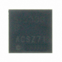
SI5338B-A-GM Silicon Laboratories Inc, SI5338B-A-GM Datasheet - Page 34

SI5338B-A-GM
Manufacturer Part Number
SI5338B-A-GM
Description
IC CLK GEN QUAD 350MHZ 24-QFN
Manufacturer
Silicon Laboratories Inc
Type
Clock Generatorr
Datasheet
1.SI5338B-A-GM.pdf
(42 pages)
Specifications of SI5338B-A-GM
Pll
Yes
Input
CML, HCSL, HSCL, LVDS, LVPECL, Crystal
Output
CMOS, HCSL. HSTL. LVDS. LVPECL. SSTL
Number Of Circuits
1
Ratio - Input:output
3:4
Differential - Input:output
Yes/Yes
Frequency - Max
350MHz
Divider/multiplier
Yes/Yes
Voltage - Supply
1.71 V ~ 3.63 V
Operating Temperature
-40°C ~ 85°C
Mounting Type
Surface Mount
Package / Case
24-QFN
Frequency-max
350MHz
Lead Free Status / RoHS Status
Lead free / RoHS Compliant
For Use With
336-1747 - KIT PROG FIELD SI5338/4/0336-1556 - BOARD EVALUATION SI5338
Lead Free Status / Rohs Status
Lead free / RoHS Compliant
Other names
336-1554-5
Available stocks
Company
Part Number
Manufacturer
Quantity
Price
Company:
Part Number:
SI5338B-A-GM
Manufacturer:
Silicon Labs
Quantity:
135
Si5338
34
Pin #
GND
PAD
15
16
17
18
19
20
21
22
23
24
RSVD_GND
Pin Name
VDDO2
VDDO1
VDDO0
CLK1B
CLK1A
CLK0B
CLK0A
GND
VDD
SDA
GND
GND
VDD
VDD
VDD
VDD
I/O
I/O
O
O
O
O
Table 15. Si5338 Pin Descriptions (Continued)
Signal Type
LVCMOS
Supply
Supply
Supply
Supply
GND
GND
Multi
Multi
Multi
Multi
Output Clock Supply Voltage.
Supply voltage (3.3, 2.5, 1.8, or 1.5 V) for CLK2A,B.
A 0.1 µF capacitor must be located very close to this pin. If CLK2 is
not used, this pin must be tied to VDD (pin 7, 24).
Output Clock Supply Voltage.
Supply voltage (3.3, 2.5, 1.8, or 1.5 V) for CLK1A,B.
A 0.1 µF capacitor must be located very close to this pin. If CLK1 is
not used, this pin must be tied to VDD (pin 7, 24).
Output Clock B for Channel 1.
May be a single-ended output or half of a differential output with
CLK1A being the other differential half. If unused, leave this pin
floating.
Output Clock A for Channel 1.
May be a single-ended output or half of a differential output with
CLK1B being the other differential half. If unused, leave this pin
floating.
I
This is the serial data for the I
required. Typical values would be 1–4 k. See the I
for more information. This pin is 3.3 V tolerant regardless of the
other supply voltages on pins 7, 11, 15, 16, 20, 24. See Register
27.
Output Clock Supply Voltage.
Supply voltage (3.3, 2.5, 1.8, or 1.5 V) for CLK0A,B.
A 0.1 µF capacitor must be located very close to this pin. If CLK0 is
not used, this pin must be tied to VDD (pin 7, 24).
Output Clock B for Channel 0.
May be a single-ended output or half of a differential output with
CLK0A being the other differential half. If unused, leave this pin
floating.
Output Clock A for Channel 0.
May be a single-ended output or half of a differential output with
CLK0B being the other differential half. If unused, leave this pin
floating.
Ground.
Must be connected to system ground. Minimize the ground path
impedance for optimal performance of this device.
Core Supply Voltage.
The device operates from a 1.8, 2.5, or 3.3 V supply. A 0.1 µF
bypass capacitor should be located very close to this pin.
Ground Pad.
This is the large pad in the center of the package. Device
specifications cannot be guaranteed unless the ground pad is
properly connected to a ground plane on the PCB. See Table 18,
“PCB Land Pattern,” on page 38 for ground via requirements.
2
C Serial Data.
Rev. 1.0
Description
2
C bus. A pullup resistor at this pin is
2
C bus spec


