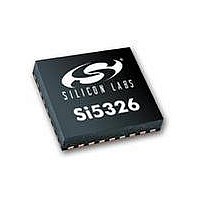
SI5326A-C-GM Silicon Laboratories Inc, SI5326A-C-GM Datasheet - Page 5

SI5326A-C-GM
Manufacturer Part Number
SI5326A-C-GM
Description
IC ANY-RATE MULTI/ATTEN 36-QFN
Manufacturer
Silicon Laboratories Inc
Type
Clock Multiplierr
Datasheet
1.SI5326B-C-GM.pdf
(72 pages)
Specifications of SI5326A-C-GM
Package / Case
36-QFN
Pll
Yes
Input
Clock
Output
CML, CMOS, LVDS, LVPECL
Number Of Circuits
1
Ratio - Input:output
2:2
Differential - Input:output
Yes/Yes
Frequency - Max
1.4GHz
Divider/multiplier
Yes/Yes
Voltage - Supply
1.71 V ~ 3.63 V
Operating Temperature
-40°C ~ 85°C
Mounting Type
Surface Mount
Frequency-max
1.4GHz
Max Input Freq
710 MHz
Max Output Freq
945 MHz
Maximum Operating Temperature
+ 85 C
Minimum Operating Temperature
- 40 C
Mounting Style
SMD/SMT
Number Of Outputs
2
Supply Current
251 mA
Supply Voltage (max)
3.3 V
Supply Voltage (min)
1.8 V
Lead Free Status / RoHS Status
Lead free / RoHS Compliant
Lead Free Status / RoHS Status
Lead free / RoHS Compliant, Lead free / RoHS Compliant
Available stocks
Company
Part Number
Manufacturer
Quantity
Price
Part Number:
SI5326A-C-GMR
Manufacturer:
SILICON LABS/èٹ¯ç§‘
Quantity:
20 000
Table 2. DC Characteristics
(V
Supply Current
CKINn Input Pins
Input Common Mode
Voltage (Input Thresh-
old Voltage)
Input Resistance
Single-Ended Input
Voltage Swing
(See Absolute Specs)
Differential Input
Voltage Swing
(See Absolute Specs)
Output Clocks (CKOUTn)
Common Mode
Notes:
DD
1.
2. No under- or overshoot is allowed.
3. LVPECL outputs require nominal V
4. This is the amount of leakage that the 3-Level inputs can tolerate from an external driver. See Si53xx
5. LVPECL, CML, LVDS and low-swing LVDS measured with Fo = 622.08 MHz.
= 1.8 ± 5%, 2.5 ±10%, or 3.3 V ±10%, T
Parameter
Current draw is independent of supply voltage
Family Reference Manual for more details.
1
2
CKO
Symbol
CKN
3
V
V
V
I
DD
ICM
ISE
ID
VCM
RIN
LVPECL 100 load line-
A
Both CKOUTs Enabled
Both CKOUTs Enabled
= –40 to 85 °C)
DD
fCKIN > 212.5 MHz
1 CKOUT Enabled
1 CKOUT Enabled
f
f
f
CKIN
CKIN
CKIN
622.08 MHz Out
622.08 MHz Out
LVPECL Format
LVPECL Format
Test Condition
19.44 MHz Out
19.44 MHz Out
CMOS Format
CMOS Format
Disable Mode
≥ 2.5 V.
See Figure 1.
See Figure 1.
See Figure 1.
See Figure 1.
Single-ended
2.5 V ± 10%
3.3 V ± 10%
1.8 V ± 5%
< 212.5 MHz
> 212.5 MHz
< 212.5 MHz
to-line
Rev. 1.0
V
0.25
0.25
1.42
Min
0.9
1.1
0.2
0.2
DD
20
—
—
—
—
—
1
–
Typ
251
217
204
194
165
40
—
—
—
—
—
—
—
—
V
DD
Max
1.95
279
243
234
220
1.4
1.7
60
—
—
—
—
—
–1.25
Si5326
Unit
V
V
V
V
mA
mA
mA
mA
mA
kΩ
V
V
V
V
PP
PP
PP
PP
5


