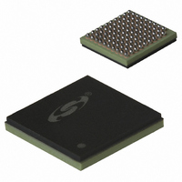
SI5364-G-BC Silicon Laboratories Inc, SI5364-G-BC Datasheet - Page 26

SI5364-G-BC
Manufacturer Part Number
SI5364-G-BC
Description
IC PREC PORT CARD CLOCK 99CBGA
Manufacturer
Silicon Laboratories Inc
Type
Clock Generatorr
Datasheet
1.SI5364-H-GL.pdf
(38 pages)
Specifications of SI5364-G-BC
Package / Case
99-CBGA
Pll
Yes
Input
Clock
Output
CML
Number Of Circuits
1
Ratio - Input:output
3:4
Differential - Input:output
Yes/Yes
Frequency - Max
675MHz
Divider/multiplier
No/Yes
Voltage - Supply
3.135 V ~ 3.465 V
Operating Temperature
-20°C ~ 85°C
Mounting Type
Surface Mount
Frequency-max
675MHz
Mounting Style
SMD/SMT
Operating Supply Voltage
2.3 V to 3.3 V
Lead Free Status / RoHS Status
Contains lead / RoHS non-compliant
Other names
336-1280
Available stocks
Company
Part Number
Manufacturer
Quantity
Price
Company:
Part Number:
SI5364-G-BC
Manufacturer:
LATTICE
Quantity:
190
Company:
Part Number:
SI5364-G-BC
Manufacturer:
SILICON
Quantity:
748
Company:
Part Number:
SI5364-G-BC
Manufacturer:
Silicon Laboratories Inc
Quantity:
10 000
Part Number:
SI5364-G-BC
Manufacturer:
SILICON LABS/èٹ¯ç§‘
Quantity:
20 000
Si5364
26
*Note: The LVTTL inputs on the Si5364 device have an internal pulldown mechanism that causes the input to default to a logic
Pin #
D10
A5
A6
B9
B5
A4
B4
low state if the input is not driven from an external source.
MANCNTRL[0]
MANCNTRL[1]
DSBLFOS
Pin Name
SMC/S3N
FOS_A
FOS_B
LOS_F
Table 10. Pin Descriptions (Continued)
I/O
O
O
O
I*
I*
I*
Signal Level
LVTTL
LVTTL
LVTTL
LVTTL
LVTTL
LVTTL
Rev. 2.5
Loss-of-Signal (LOS) Alarm for REF/CLKIN_F.
See LOS_A.
Frequency Offset (FOS) Alarm for CLKIN_A.
Active high output indicates that the frequency offset
between CLKIN_A and REF/CLKIN_F exceeds the
selectable frequency offset threshold. The offset
threshold is selected by the SMC/S3N input. This
output can be disabled with the DSBLFOS control
input.
Frequency Offset (FOS) Alarm for CLKIN_B.
See FOS_A.
SONET Minimum Clock/Stratum3-3E.
Sets the frequency offset threshold used to trigger
the FOS_A and FOS_B alarm outputs.
0 = 9.2–16.6 ppm for Stratum 3/3E operation.
1 = 40–72 ppm for SONET Minimum Clock opera-
tion.
Disable FOS.
When high, all frequency offset comparison and error
generation functionality is disabled. When Disable
FOS is active, the FOS_A and FOS_B outputs are
low, and automatic switching is based only on loss-
of-signal (LOS) status.
Manual Switching Control.
Selects the input clock used by the DSPLL to gener-
ate the SONET/SDH clock outputs. Selection of digi-
tal hold mode locks the current state of the DSPLL
and forces the DSPLL to continue generation of the
output clocks with no additional phase or frequency
information from the input clocks. The MANCNTRL
inputs are internally deglitched to prevent inadvertent
clock switching during changes in the MANCNTRL
state.
The MANCNTRL[1:0] inputs are decoded as follows:
00 = Manual selection of REF/CLKIN_F.
01 = Manual selection of CLKIN_B.
10 = Manual selection of CLKIN_A.
11 = Digital hold mode.
The MANCNTRL inputs are ignored when the AUTO-
SEL input is high.
Description


