MAXQ3181-RAN+ Maxim Integrated Products, MAXQ3181-RAN+ Datasheet - Page 22

MAXQ3181-RAN+
Manufacturer Part Number
MAXQ3181-RAN+
Description
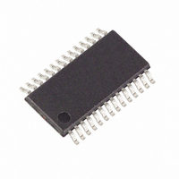
IC AFE POLYPHASE LO-PWR 28-TSSOP
Manufacturer
Maxim Integrated Products
Datasheet
1.MAXQ3181-RAN.pdf
(84 pages)
Specifications of MAXQ3181-RAN+
Number Of Channels
8
Power (watts)
35mW
Voltage - Supply, Analog
3.3V
Voltage - Supply, Digital
3.3V
Package / Case
28-TSSOP
Lead Free Status / RoHS Status
Lead free / RoHS Compliant
Number Of Bits
-
Low-Power, Active Energy, Polyphase AFE
The length of the transfer is defined by the first com-
mand byte and the status of the CRCEN bit in the
OPMODE1 register. There is no special synchronization
mechanism provided in this simple protocol. Therefore,
the master is responsible for sending/receiving the cor-
rect number of bytes. If the master mistakenly sends
more bytes than are required by the current command,
the extra bytes are either ignored (if the MAXQ3181 is
busy processing the previous command) or are inter-
preted as the beginning of a new command. If the mas-
ter sends fewer bytes than are required by the current
command, the MAXQ3181 waits for SPI timeout, then
drops the transaction and resets the communication
channel. The duration of the timeout can be configured
through the COM_TIMO register.
Figures 5 and 6 show typical 2-byte reading and writing
transfers (without CRC byte).
Figure 5. Read SPI Transfer
Figure 6. Write SPI Transfer
22
______________________________________________________________________________________
SCLK
MOSI
MISO
SCLK
MOSI
MISO
SSEL
SSEL
00 01
10 01
0xC1
0xC1
ADDRESS
ADDRESS
0xC2
0xC2
WRITING DATA TO MAXQ3181 THROUGH SPI INTERFACE
READING DATA FROM MAXQ3181 THROUGH SPI INTERFACE
NACK (0x4E)
ACK (0x41)
DATA LSB
DUMMY
Individual message bytes sent through the SPI are
processed in a software routine contained in the ROM
firmware. For this reason, it is necessary to provide a
delay between successive bytes. This byte spacing
must be no less than 400 system clocks to ensure that
the MAXQ3181 has a chance to read and process the
byte before the arrival of the next one. It is strongly rec-
ommended that CRC be enabled for both read and
write to achieve reliable communications.
Data and device command and control information are
located in internal registers. Registers range from 8 to
64 bits in length and are divided into RAM-based regis-
ters and virtual registers. The RAM-based registers
contain both operating parameters and measurement
results.
ACK (0x41)
DATA MSB
ACK (0x41)
DUMMY
NACK (0x4E)
DATA LSB
DUMMY
DUMMY
Host Software Design
ACK (0x41)
DATA MSB
DUMMY
DUMMY
Register Set


