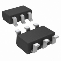
ADC101S101CIMF/NOPB National Semiconductor, ADC101S101CIMF/NOPB Datasheet - Page 11

ADC101S101CIMF/NOPB
Manufacturer Part Number
ADC101S101CIMF/NOPB
Description
IC ADC 10BIT 1MSPS SOT23-6
Manufacturer
National Semiconductor
Series
PowerWise®r
Datasheet
1.ADC101S101CIMFNOPB.pdf
(16 pages)
Specifications of ADC101S101CIMF/NOPB
Number Of Bits
10
Sampling Rate (per Second)
1M
Data Interface
DSP, MICROWIRE™, QSPI™, Serial, SPI™
Number Of Converters
1
Power Dissipation (max)
10mW
Voltage Supply Source
Single Supply
Operating Temperature
-40°C ~ 85°C
Mounting Type
Surface Mount
Package / Case
SOT-23-6
Number Of Elements
1
Resolution
10Bit
Architecture
SAR
Sample Rate
1MSPS
Input Polarity
Unipolar
Input Type
Voltage
Rated Input Volt
5.25V
Differential Input
No
Power Supply Requirement
Single
Single Supply Voltage (typ)
3.3/5V
Single Supply Voltage (min)
2.7V
Single Supply Voltage (max)
5.25V
Dual Supply Voltage (typ)
Not RequiredV
Dual Supply Voltage (min)
Not RequiredV
Dual Supply Voltage (max)
Not RequiredV
Differential Linearity Error
±0.7LSB
Integral Nonlinearity Error
±0.7LSB
Operating Temp Range
-40C to 85C
Operating Temperature Classification
Industrial
Mounting
Surface Mount
Pin Count
6
Package Type
SOT-23
Input Signal Type
Single-Ended
For Use With
ADC101S101EVAL - BOARD EVALUATION FOR ADC101S101
Lead Free Status / RoHS Status
Lead free / RoHS Compliant
Other names
ADC101S101CIMF
ADC101S101CIMFTR
ADC101S101CIMFTR
Applications Information
1.0 ADC101S101 OPERATION
The ADC101S101 is a successive-approximation analog-to-
digital converter designed around a charge-redistribution dig-
ital-to-analog converter core. Simplified schematics of the
ADC101S101 in both track and hold operation are shown in
Figures 3 and 4, respectively. In Figure 3, the device is in track
mode: switch SW1 connects the sampling capacitor to the in-
put, and SW2 balances the comparator inputs. The device is
in this state until CS is brought low, at which point the device
moves to the hold mode.
2.0 USING THE ADC101S101
The serial interface timing diagram for the ADC is shown in
Figure 2. CS is chip select, which initiates conversions on the
ADC and frames the serial data transfers. SCLK (serial clock)
controls both the conversion process and the timing of serial
data. SDATA is the serial data out pin, where a conversion
result is found as a serial data stream.
Basic operation of the ADC begins with CS going low, which
initiates a conversion process and data transfer. Subsequent
rising and falling edges of SCLK will be labelled with reference
to the falling edge of CS; for example, "the third falling edge
of SCLK" shall refer to the third falling edge of SCLK after
CS goes low.
At the fall of CS, the SDATA pin comes out of TRI-STATE,
and the converter moves from track mode to hold mode. The
input signal is sampled and held for conversion on the falling
edge of CS. The converter moves from hold mode to track
mode on the 13th rising edge of SCLK (see
this point that the interval for the T
the worst case, 350 ns must pass between the 13th rising
ACQ
specification begins. In
FIGURE 3. ADC101S101 in Track Mode
FIGURE 4. ADC101S101 in Hold Mode
Figure
2). It is at
11
Figure 4 shows the device in hold mode: switch SW1 con-
nects the sampling capacitor to ground, maintaining the sam-
pled voltage, and switch SW2 unbalances the comparator.
The control logic then instructs the charge-redistribution DAC
to add or subtract fixed amounts of charge from the sampling
capacitor until the comparator is balanced. When the com-
parator is balanced, the digital word supplied to the DAC is
the digital representation of the analog input voltage. The de-
vice moves from hold mode to track mode on the 13th rising
edge of SCLK.
edge and the next falling edge of SCLK. The SDATA pin will
be placed back into TRI-STATE after the 16th falling edge of
SCLK, or at the rising edge of CS, whichever occurs first. After
a conversion is completed, the quiet time t
isfied before bringing CS low again to begin another conver-
sion.
Sixteen SCLK cycles are required to read a complete sample
from the ADC. The sample bits (including leading or trailing
zeroes) are clocked out on falling edges of SCLK, and are
intended to be clocked in by a receiver on subsequent falling
edges of SCLK. The ADC will produce three leading zero bits
on SDATA, followed by ten data bits, most significant first.
After the data bits, the ADC will clock out two trailing zeros.
If CS goes low before the rising edge of SCLK, an additional
(fourth) zero bit may be captured by the next falling edge of
SCLK.
2.1 Determining Throughput
Throughput depends on the frequency of SCLK and how
much time is allowed to elapse between the end of one con-
20145209
20145210
QUIET
must be sat-
www.national.com


