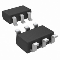
ADC101S101CIMF/NOPB National Semiconductor, ADC101S101CIMF/NOPB Datasheet - Page 3

ADC101S101CIMF/NOPB
Manufacturer Part Number
ADC101S101CIMF/NOPB
Description
IC ADC 10BIT 1MSPS SOT23-6
Manufacturer
National Semiconductor
Series
PowerWise®r
Datasheet
1.ADC101S101CIMFNOPB.pdf
(16 pages)
Specifications of ADC101S101CIMF/NOPB
Number Of Bits
10
Sampling Rate (per Second)
1M
Data Interface
DSP, MICROWIRE™, QSPI™, Serial, SPI™
Number Of Converters
1
Power Dissipation (max)
10mW
Voltage Supply Source
Single Supply
Operating Temperature
-40°C ~ 85°C
Mounting Type
Surface Mount
Package / Case
SOT-23-6
Number Of Elements
1
Resolution
10Bit
Architecture
SAR
Sample Rate
1MSPS
Input Polarity
Unipolar
Input Type
Voltage
Rated Input Volt
5.25V
Differential Input
No
Power Supply Requirement
Single
Single Supply Voltage (typ)
3.3/5V
Single Supply Voltage (min)
2.7V
Single Supply Voltage (max)
5.25V
Dual Supply Voltage (typ)
Not RequiredV
Dual Supply Voltage (min)
Not RequiredV
Dual Supply Voltage (max)
Not RequiredV
Differential Linearity Error
±0.7LSB
Integral Nonlinearity Error
±0.7LSB
Operating Temp Range
-40C to 85C
Operating Temperature Classification
Industrial
Mounting
Surface Mount
Pin Count
6
Package Type
SOT-23
Input Signal Type
Single-Ended
For Use With
ADC101S101EVAL - BOARD EVALUATION FOR ADC101S101
Lead Free Status / RoHS Status
Lead free / RoHS Compliant
Other names
ADC101S101CIMF
ADC101S101CIMFTR
ADC101S101CIMFTR
STATIC CONVERTER CHARACTERISTICS
INL
DNL
V
GE
DYNAMIC CONVERTER CHARACTERISTICS
SINAD
SNR
THD
SFDR
ENOB
IMD
FPBW
Symbol
OFF
Absolute Maximum Ratings
2)
If Military/Aerospace specified devices are required,
please contact the National Semiconductor Sales Office/
Distributors for availability and specifications.
ADC101S101 Converter Electrical Characteristics
The following specifications apply for V
f
Analog Supply Voltage V
Voltage on Any Pin to GND
Input Current at Any Pin
Package Input Current
Power Consumption at T
ESD Susceptibility
Junction Temperature
Storage Temperature
SAMPLE
Human Body Model
Machine Model
= 500 ksps to 1 Msps, unless otherwise noted. Boldface limits apply for T
Resolution with No Missing Codes
Integral Non-Linearity
Differential Non-Linearity
Offset Error
Gain Error
Signal-to-Noise Plus Distortion Ratio
Signal-to-Noise Ratio
Total Harmonic Distortion
Spurious-Free Dynamic Range
Effective Number of Bits
Intermodulation Distortion, Second
Order Terms
Intermodulation Distortion, Third Order
Terms
-3 dB Full Power Bandwidth
(Note
Parameter
(Note
(Note
A
A
5)
= 25°C
3)
3)
A
−0.3V to (V
= +2.7V to 5.25V, GND = 0V, f
−65°C to +150°C
−0.3V to 6.5V
(Note
See
V
V
V
V
V
f
V
f
V
f
V
f
V
f
V
f
V
f
V
V
IN
IN
IN
IN
IN
a
a
A
A
A
A
A
A
A
A
A
A
A
A
A
= 103.5 kHz, f
= 103.5 kHz, f
= 100 kHz, −0.02 dBFS
= 100 kHz, −0.02 dBFS
= 100 kHz, −0.02 dBFS
= 100 kHz, −0.02 dBFS
= 100 kHz, −0.02 dBFS
= +2.7V to +5.25V
= +2.7V to +5.25V
= +2.7V to +5.25V
= +2.7V to +5.25V
= +2.7 to 5.25V
= +2.7 to 5.25V
= +2.7 to 5.25V
= +2.7 to 5.25V
= +2.7 to 5.25V
= +5.25V
= +5.25V
= +5V
= +3V
A
(Note
±10 mA
±20 mA
+150°C
1,
+0.3)V
3500V
300V
Note
4)
Conditions
3
b
b
= 113.5 kHz
= 113.5 kHz
Operating Ratings
Package Thermal Resistance
Soldering
Semiconductor's Reflow Temperature Profile specifications.
Refer to www.national.com/packaging.
Operating Temperature Range
V
Digital Input Pins Voltage Range
Clock Frequency
Sample Rate
Analog Input Voltage
A
SCLK
Supply Voltage
(regardless of supply voltage)
= 10 MHz to 20 MHz, C
6-lead SOT-23
process
6-lead LLP
A
Package
= T
(Note
MIN
7,
to T
Typical
must
±0.2
+0.3
−0.2
±0.1
±0.2
61.7
Note
−77
−78
−78
9.9
62
78
11
8
MAX
9)
L
: all other limits T
(Note
= 15 pF,
comply
(Note
Limits
±0.7
±0.7
±0.7
±1.0
61.2
265°C / W
−73
9.8
94°C / W
10
61
74
1,
−40°C
(Note
θ
Note
9)
25 kHz to 20 MHz
JA
+2.7V to +5.25V
−0.3V to +5.25V
with
6)
≤
2)
up to 1 Msps
T
www.national.com
A
LSB (max)
LSB (max)
LSB (max)
LSB (min)
LSB (min)
Bits (min)
dB (max)
A
dB (min)
dB (min)
dB (min)
= 25°C.
≤
0V to V
Units
MHz
MHz
National
Bits
dB
dB
+85°C
A


