HI5812JIPZ Intersil, HI5812JIPZ Datasheet
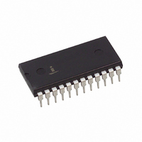
IC ADC 12BIT 50KSPS LP HS 24DIP

HI5812JIPZ

Manufacturer Part Number
HI5812JIPZ
Description
IC ADC 12BIT 50KSPS LP HS 24DIP
Manufacturer
Intersil
Datasheet

Specifications of HI5812JIPZ

Number Of Bits
12
Sampling Rate (per Second)
50k
Data Interface
Parallel
Number Of Converters
1
Power Dissipation (max)
25mW
Voltage Supply Source
Analog and Digital
Operating Temperature
-40°C ~ 85°C
Mounting Type
Through Hole
Package / Case
24-DIP (0.300", 7.62mm)
Lead Free Status / RoHS Status
Lead free / RoHS Compliant
CMOS 20 Microsecond, 12-Bit, Sampling
A/D Converter with Internal Track and
Hold
The HI5812 is a fast, low power, 12-bit, successive
approximation analog-to-digital converter. It can operate
from a single 3V to 6V supply and typically draws just 1.9mA
when operating at 5V. The HI5812 features a built-in track
and hold. The conversion time is as low as 20µs with a 5V
supply.
The twelve data outputs feature full high speed CMOS
three-state bus driver capability, and are latched and held
through a full conversion cycle. The output is user
selectable, i.e., 12-bit, 8-bit (MSBs), and/or 4-bit (LSBs). A
data ready flag, and conversion-start input complete the
digital interface.
An internal clock is provided and is available as an output.
The clock may also be over-driven by an external source.
Ordering Information
HI5812JIP
HI5812JIPZ
(See Note)
HI5812JIB
HI5812JIBZ
(See Note)
HI5812KIB
HI5812KIBZ
(See Note)
*Pb-free PDIPs can be used for through hole wave solder
processing only. They are not intended for use in Reflow solder
processing applications.
NOTE: Intersil Pb-free products employ special Pb-free material
sets; molding compounds/die attach materials and 100% matte tin
plate termination finish, which are RoHS compliant and compatible
with both SnPb and Pb-free soldering operations. Intersil Pb-free
products are MSL classified at Pb-free peak reflow temperatures that
meet or exceed the Pb-free requirements of IPC/JEDEC J STD-020.
NUMBER
PART
(MAX OVER
INL (LSB)
TEMP.)
±1.5
±1.5
±1.5
±1.5
±1.0
±1.0
®
-40 to 85 24 Ld PDIP
-40 to 85 24 Ld PDIP*
-40 to 85 24 Ld SOIC
RANGE
TEMP.
(
1
o
C)
Data Sheet
(Pb-free)
(Pb-free)
(Pb-free)
PACKAGE
E24.3
E24.3
M24.3
M24.3
M24.3
M24.3
DWG. #
PKG.
1-888-INTERSIL or 1-888-352-6832
CAUTION: These devices are sensitive to electrostatic discharge; follow proper IC Handling Procedures.
Features
• Conversion Time . . . . . . . . . . . . . . . . . . . . . . . . . . . 20µs
• Throughput Rate . . . . . . . . . . . . . . . . . . . . . . . . 50 kSPS
• Built-In Track and Hold
• Guaranteed No Missing Codes Over Temperature
• Single Supply Voltage . . . . . . . . . . . . . . . . . . . . . . . . .+5V
• Maximum Power Consumption. . . . . . . . . . . . . . . . 25mW
• Internal or External Clock
• Pb-Free Available (RoHS Compliant)
Applications
• Remote Low Power Data Acquisition Systems
• Digital Audio
• DSP Modems
• General Purpose DSP Front End
• µP Controlled Measurement System
• Professional Audio Positioner/Fader
Pinout
March 31, 2005
All other trademarks mentioned are the property of their respective owners.
|
(LSB) D0
Intersil (and design) is a registered trademark of Intersil Americas Inc.
DRDY
V
Copyright Intersil Americas Inc. 2001, 2005. All Rights Reserved
SS
D1
D2
D3
D4
D5
D6
D7
D8
D9
10
11
12
1
2
3
4
5
6
7
8
9
(PDIP, SOIC)
TOP VIEW
HI5812
24
23
22
21
20
19
18
17
16
15
14
13
V
CLK
STRT
V
V
V
OEM
D11 (MSB)
D10
OEL
V
V
AA
DD
REF
REF
AA
IN
+
-
+
-
HI5812
FN3214.6

Related parts for HI5812JIPZ

HI5812JIPZ Summary of contents

Page 1

... The clock may also be over-driven by an external source. Ordering Information INL (LSB) TEMP. PART (MAX OVER RANGE o NUMBER TEMP ±1.5 HI5812JIP - PDIP ±1.5 HI5812JIPZ - PDIP* (See Note) (Pb-free) ±1.5 HI5812JIB - SOIC ±1.5 HI5812JIBZ - SOIC (See Note) (Pb-free) ±1.0 HI5812KIB - SOIC ±1.0 ...

Page 2

Functional Block Diagram INTERNAL LOGIC REF 50Ω SUBSTRATE 32C AA 64C 63 16C REF 2 HI5812 CONTROL ...

Page 3

Absolute Maximum Ratings Supply Voltage ...

Page 4

Electrical Specifications Unless Otherwise Specified (Continued) PARAMETER Spurious Free Dynamic Range, SFDR ANALOG INPUT Input Current, Dynamic Input Current, Static Input Bandwidth -3dB Reference Input Current Input Series Resistance Input Capacitance, C SAMPLE Input ...

Page 5

Electrical Specifications Unless Otherwise Specified (Continued) PARAMETER Clock Delay from Start, t STRT D Output Enable Delay Output Disabled Delay, t DIS POWER SUPPLY CHARACTERISTICS Supply Current NOTE: 2. ...

Page 6

Timing Diagrams (Continued) 15 CLK (EXTERNAL) STRT DRDY HOLD CLK (INTERNAL) STRT DRDY HOLD HI5812 STRT R TRACK FIGURE 2. SINGLE SHOT MODE EXTERNAL CLOCK STRT ...

Page 7

Timing Diagrams (Continued) OEL OR OEM D11 HIGH IMPEDANCE TO HIGH HIGH IMPEDANCE 50% TO LOW FIGURE 4A. 7 HI5812 t DIS 90% TO OUTPUT PIN 10% FIGURE 4. OUTPUT ENABLE/DISABLE ...

Page 8

Typical Performance Curves 1 5V 4.608V DD AA REF 0.75 0.5 0.25 A. CLK = INTERNAL B. CLK = 750kHz C. CLK = 1MHz 0 -60 - -40 TEMPERATURE ...

Page 9

Typical Performance Curves 5V 4.608V DD AA REF -60 -40 - TEMPERATURE ( FIGURE 12. SUPPLY CURRENT vs TEMPERATURE ...

Page 10

TABLE 1. PIN DESCRIPTIONS PIN NO. NAME DESCRIPTION 1 DRDY Output flag signifying new data is available. Goes high at end of clock period 15. Goes low when new conversion is started Bit 0 (Least Significant Bit, LSB). ...

Page 11

A simplified analog input model is presented in Figure 19. During tracking, the A/D input (V ) typically appears 380pF capacitor being charged through a 420Ω internal switch resistance. The time constant is 160ns. To charge this ...

Page 12

Depending on how long the clock was shut off, the low portion of clock period 2 may be longer than during the remaining cycles. The input will continue to track until the end of period 3, the same as when ...

Page 13

Effective Number of Bits The effective number of bits (ENOB) is derived from the SINAD data; SINAD - 1.76 ENOB = 6.02 Total Harmonic Distortion The total harmonic distortion (THD) is the ratio of the RMS sum of the second ...

Page 14

Die Characteristics DIE DIMENSIONS: 3200µm x 3940µm METALLIZATION: Type: AlSi ±1k Å Å Thickness: 11k Metallization Mask Layout HI5812 PASSIVATION: Type: PSG Thickness: 13k WORST CASE CURRENT DENSITY: 1. ...

Page 15

Dual-In-Line Plastic Packages (PDIP INDEX N/2 AREA -B- -A- D BASE PLANE -C- SEATING PLANE 0.010 (0.25 NOTES: 1. Controlling Dimensions: INCH. In case of conflict between ...

Page 16

... Accordingly, the reader is cautioned to verify that data sheets are current before placing orders. Information furnished by Intersil is believed to be accurate and reliable. However, no responsibility is assumed by Intersil or its subsidiaries for its use; nor for any infringements of patents or other rights of third parties which may result from its use ...

Related keywords