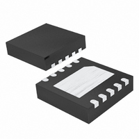
MAX1396ETB+T Maxim Integrated Products, MAX1396ETB+T Datasheet - Page 9

MAX1396ETB+T
Manufacturer Part Number
MAX1396ETB+T
Description
IC ADC 12BIT 312.5KSPS 10-TDFN
Manufacturer
Maxim Integrated Products
Datasheet
1.MAX1396ETBT.pdf
(18 pages)
Specifications of MAX1396ETB+T
Number Of Bits
12
Sampling Rate (per Second)
312.5k
Data Interface
DSP, MICROWIRE™, QSPI™, Serial, SPI™
Number Of Converters
1
Power Dissipation (max)
830µW
Voltage Supply Source
Single Supply
Operating Temperature
-40°C ~ 85°C
Mounting Type
Surface Mount
Package / Case
10-WFDFN Exposed Pad
Number Of Adc Inputs
2
Architecture
SAR
Conversion Rate
312 KSPs
Resolution
12 bit
Interface Type
Serial
Voltage Reference
External
Supply Voltage (max)
3.3 V
Mounting Style
SMD/SMT
Lead Free Status / RoHS Status
Lead free / RoHS Compliant
Other names
MAX1396ETB+T
1.5V to 3.6V, 312.5ksps, 1-Channel True-Differential/
and the difference between the sampled positive and
negative input voltages is converted. The time required
for the T/H to acquire an input signal is determined by
how quickly its input capacitance is charged. The
required acquisition time lengthens as the input signal’s
source impedance increases. The acquisition time,
t
acquired. It is calculated by the following equation:
where:
R
R
input resistance.
C
input capacitance.
t
Note: t
impedance below 400Ω does not significantly affect the
ADC’s AC performance.
Figure 4. Equivalent Input Circuit
ACQ
PU
SOURCE
IN
IN
*INDICATES THE MAX1393
= 400ns.
= 500Ω, which is the equivalent differential analog
= 16pF, which is the equivalent differential analog
, is the minimum time needed for the signal to be
R
SOURCE
ANALOG
SIGNAL
SOURCE
ACQ
t
ACQ
is the source impedance of the input signal.
is never less than 600ns and any source
≥ 9 x (R
GND (AIN-)*
A
IN
1 (AIN+)*
_______________________________________________________________________________________
AIN2
2-Channel Single-Ended, 12-Bit, SAR ADCs
HOLD
SOURCE
GND
REF
V
HOLD
DD
+ R
CIN+
CIN-
/2
RIN-
IN
) x C
DAC
TRACK
IN
COMPARATOR
RIN+
+ t
MAX1393
MAX1396
+
-
HOLD
PU
The ADC’s input-tracking circuitry has a 4MHz full-
power bandwidth, making it possible to digitize high-
speed transient events and measure periodic signals
with bandwidths exceeding the ADC’s sampling rate by
using undersampling techniques.
Use anti-alias filtering to avoid high-frequency signals
being aliased into the frequency band of interest.
The MAX1393/MAX1396 produce a digital output that
corresponds to the analog input voltage as long as the
analog inputs are within their specified range. When
operating the MAX1393 in unipolar mode (UNI/BIP = 1),
the specified differential analog input range is from 0 to
V
the differential analog input range is from -V
+V
MAX1396 has an input range from 0 to V
Internal protection diodes confine the analog input volt-
age within the region of the analog power input rails
(V
from GND - 0.3V to V
voltages beyond GND - 0.3V and V
bias the internal protection diodes. In this situation, limit
the forward diode current to less than 50mA to avoid
damage to the MAX1393/MAX1396.
Figures 8, 9, and 10 illustrate the conversion timing for
the MAX1393/MAX1396. Sixteen SCLK cycles are
required to read the conversion result and data on
DOUT transitions on the falling edge of SCLK. The con-
version result contains 4 zeros, followed by 12 data bits
with the data in MSB-first format. For the MAX1393, data
is straight binary for unipolar mode and two’s comple-
ment for bipolar mode. For the MAX1396, data is always
straight binary.
Figure 5 shows the unipolar transfer function for the
MAX1393/MAX1396. Figure 6 shows the bipolar trans-
fer function for the MAX1393. Code transitions occur
halfway between successive-integer LSB values.
REF
DD
REF
. When operating in bipolar mode (UNI/BIP = 0),
, GND) and allow the analog input voltage to swing
/2 with a common-mode range of 0 to V
Analog Input Range and Protection
DD
Analog Input Bandwidth
+ 0.3V without damage. Input
Output Data Format
Transfer Function
DD
REF
+ 0.3V forward
.
REF
DD
. The
/2 to
9


