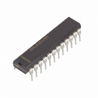
MAX191BCNG+ Maxim Integrated Products, MAX191BCNG+ Datasheet - Page 15

MAX191BCNG+
Manufacturer Part Number
MAX191BCNG+
Description
IC ADC 12BIT 100KSPS W/REF 24DIP
Manufacturer
Maxim Integrated Products
Datasheet
1.MAX191BCWG.pdf
(24 pages)
Specifications of MAX191BCNG+
Number Of Bits
12
Sampling Rate (per Second)
100k
Data Interface
MICROWIRE™, Parallel, QSPI™, Serial, SPI™
Number Of Converters
1
Power Dissipation (max)
1.07W
Voltage Supply Source
Dual ±
Operating Temperature
0°C ~ 70°C
Mounting Type
Through Hole
Package / Case
24-DIP (0.300", 7.62mm)
Number Of Adc Inputs
1
Architecture
SAR
Conversion Rate
100 KSPs
Resolution
12 bit
Input Type
Voltage
Interface Type
Serial
Voltage Reference
Internal 4.096 V or External
Supply Voltage (max)
5 V
Maximum Power Dissipation
1067 mW
Maximum Operating Temperature
+ 70 C
Mounting Style
Through Hole
Minimum Operating Temperature
0 C
Lead Free Status / RoHS Status
Lead free / RoHS Compliant
ing edge of the first clock cycle after conversion end
(when BUSY goes high). As mentioned previously, two
more read operations (after BUSY goes high) are
needed to access the conversion results. The only dif-
ference is that now the low byte can be read first. This
happens by allowing the first read operation to occur
with HBEN low, where the 8 LSBs are accessed. The
second read, with HBEN high, accesses the 4 MSBs
with 4 leading 0s.
The serial mode is compatible with Microwire, SPI and
QSPI serial interfaces. In addition, a framing signal
(SSTRB) is provided that allows the devices to interface
with the TMS320 family of DSPs. Set PAR low for serial
mode. A falling edge on CS causes the T/H to sample
the input (Figure 10). Conversion always begins on the
next falling edge of SCLK, regardless of where CS
occurs. The DOUT line remains high-impedance until a
conversion begins. During the MSB decision, DOUT
remains low (leading 0), while SSTRB goes high to indi-
cate that a data frame is beginning. The data is avail-
able at DOUT on the rising edge of SCLK (SCLK
when using an internal clock) and transitions on the
falling edge. DOUT remains low after all data bits have
been shifted out, inserting trailing 0s in the data stream
until CS returns high. The SCLK
nous with the internal or external clock.
For interface flexibility, DOUT, SCLK
signals enter a high-impedance state when CS is high.
When CS is low, RD controls the status of SCLK
SSTRB outputs. A logic low RD enables SCLK
SSTRB, while a logic high forces both outputs into a
high-impedance state. Also, with CS low and HBEN
high, SCLK
version status. This is useful with µPs that require a
Figure 12. f
the serial data input to the µP.
t
t
f
SU
22
SCLK
(M) IS THE SETUP TIME REQUIRED AT THE SERIAL DATA INPUT TO THE P.
IS THE MAXIMUM SCLK TO DOUT DELAY.
(MAX) = ––
SCLK
DOUT
SCLK
OUT
1
2
(MAX) is limited by the setup time required by
drives continuously, regardless of con-
(
with Internal Reference and Power-Down
–––––––––
t
SU
______________________________________________________________________________________
(M) + t
1
22
t
22
)
Serial-Interface Mode
OUT
t
SETUP
Low-Power, 12-Bit Sampling ADC
(MIN)
signal is synchro-
OUT
and SSTRB
OUT
OUT
and
and
OUT
continuous serial clock. If CS and HBEN are low,
SCLK
while the converter internal clock runs continuously.
This is useful for creating a simple serial-to-parallel
interface without shift-register overflow (Figure 11).
The maximum SCLK rate depends on the minimum
setup time required at the serial data input to the µP
and the ADC’s DOUT to SCLK delay (t
12). The maximum f
Figure 13. Common Serial-Interface Connections to the MAX191
a. SPI
b. QSPI
c. MICROWIRE
d. TMS320 SERIAL INTERFACE
OUT
is output only during the conversion cycle,
Maximum Clock Rate in Serial Mode
MISO
CLKX
CLKR
MISO
SCK
FSR
SCLK
SCK
CS
I/O
SK
I/O
DR
I/O
SS
SS
SI
is as follows:
+5V
+5V
SCLK
DOUT
CS
SCLK
DOUT
CS
SCLK
DOUT
CS
SCLK
SSTRB
CS
DOUT
MAX191
MAX191
MAX191
MAX191
22
) (see Figure
15


