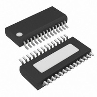
MAX1295BEEI+ Maxim Integrated Products, MAX1295BEEI+ Datasheet - Page 11

MAX1295BEEI+
Manufacturer Part Number
MAX1295BEEI+
Description
IC ADC 12BIT 265KSPS 28-QSOP
Manufacturer
Maxim Integrated Products
Datasheet
1.MAX1297BEEG.pdf
(19 pages)
Specifications of MAX1295BEEI+
Number Of Bits
12
Sampling Rate (per Second)
265k
Data Interface
Parallel
Number Of Converters
1
Power Dissipation (max)
762mW
Voltage Supply Source
Single Supply
Operating Temperature
-40°C ~ 85°C
Mounting Type
Surface Mount
Package / Case
28-QSOP
Number Of Adc Inputs
6
Architecture
SAR
Conversion Rate
265 KSPs
Resolution
12 bit
Voltage Reference
Internal 2.5 V or External
Supply Voltage (max)
3.3 V
Mounting Style
SMD/SMT
Lead Free Status / RoHS Status
Lead free / RoHS Compliant
Together with the input impedance, this capacitor
forms an RC filter, limiting the ADC’s signal bandwidth.
The MAX1295/MAX1297 T/H stage offers a 250kHz full-
linear and a 3MHz full-power bandwidth. This makes it
possible to digitize high-speed transients and measure
periodic signals with bandwidths exceeding the ADC’s
sampling rate by using undersampling techniques. To
avoid high-frequency signals being aliased into the fre-
quency band of interest, anti-alias filtering is recom-
mended.
Initiate a conversion by writing a control byte that selects
the multiplexer channel and configures the MAX1295/
MAX1297 for either unipolar or bipolar operation. A
write pulse (WR + CS) can either start an acquisition
interval or initiate a combined acquisition plus conver-
sion. The sampling interval occurs at the end of the
acquisition interval. The acquisition mode (ACQMOD)
bit in the input control byte (Table 1) offers two options
Figure 4. Conversion Timing Using Internal Acquisition Mode
CS
WR
D7–D0
RD
INT
DOUT
with +2.5V Reference and Parallel Interface
HIGH-Z
______________________________________________________________________________________
265ksps, +3V, 6-/2-Channel, 12-Bit ADCs
HIGH-Z
t
t
DS
CSWS
t
t
Starting a Conversion
WR
CS
ACQMOD = "0"
CONTROL
BYTE
Input Bandwidth
t
ACQ
t
DH
t
CSWH
t
CONV
for acquiring the signal: an internal and an external
acquisition. The conversion period lasts for 13 clock
cycles in either the internal or external clock or acquisi-
tion mode. Writing a new control byte during a conver-
sion cycle aborts the conversion and starts a new
acquisition interval.
Select internal acquisition by writing the control byte
with the ACQMOD bit cleared (ACQMOD = 0). This
causes the write pulse to initiate an acquisition interval
whose duration is internally timed. Conversion starts
when this acquisition interval (three external clock
cycles or approximately 1µs in internal clock mode)
ends (Figure 4). Note that, when the internal acquisition
is combined with the internal clock, the aperture jitter
can be as high as 200ps. Internal clock users wishing
to achieve the 50ps jitter specification should always
use external acquisition mode.
t
INT1
t
D0
DATA VALID
Internal Acquisition
HIGH-Z
HIGH-Z
t
TR
11


