MAX1295BEEI+ Maxim Integrated Products, MAX1295BEEI+ Datasheet - Page 14

MAX1295BEEI+
Manufacturer Part Number
MAX1295BEEI+
Description
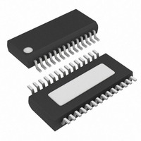
IC ADC 12BIT 265KSPS 28-QSOP
Manufacturer
Maxim Integrated Products
Datasheet
1.MAX1297BEEG.pdf
(19 pages)
Specifications of MAX1295BEEI+
Number Of Bits
12
Sampling Rate (per Second)
265k
Data Interface
Parallel
Number Of Converters
1
Power Dissipation (max)
762mW
Voltage Supply Source
Single Supply
Operating Temperature
-40°C ~ 85°C
Mounting Type
Surface Mount
Package / Case
28-QSOP
Number Of Adc Inputs
6
Architecture
SAR
Conversion Rate
265 KSPs
Resolution
12 bit
Voltage Reference
Internal 2.5 V or External
Supply Voltage (max)
3.3 V
Mounting Style
SMD/SMT
Lead Free Status / RoHS Status
Lead free / RoHS Compliant
the chip-select signal, which enables a µP to address
the MAX1295/MAX1297 as an I/O port. When high, CS
disables the CLK, WR, and RD inputs and forces the
interface into a high-impedance (high-Z) state.
The control bit sequence is latched into the device on
pins D7–D0 during a write command. Table 4 shows
the control-byte format.
The 12-bit-wide output format for both the MAX1295/
MAX1297 is binary in unipolar mode and two’s comple-
ment in bipolar mode. CS, RD, WR, INT, and the 12 bits
of output data can interface directly to a 16-bit data bus.
When reading the output data, CS and RD must be low.
When power is first applied, internal power-on reset cir-
cuitry activates the MAX1295/MAX1297 in external clock
mode and sets INT high. After the power supplies stabi-
lize, the internal reset time is 10µs; no conversions
should be attempted during this phase. When using the
internal reference, 500µs is required for V
The MAX1295/MAX1297 can be used with an internal
or external reference voltage. An external reference
can be connected directly to REF or REFADJ.
265ksps, +3V, 6-/2-Channel, 12-Bit ADCs
with +2.5V Reference and Parallel Interface
Table 4. Control-Byte Format
Figure 7. Reference Adjustment with External Potentiometer
14
__________Applications Information
50kΩ
50kΩ
(MSB)
______________________________________________________________________________________
V
PD1
D7
DD
= +3V
GND
Internal and External Reference
330kΩ
PD0
D6
0.01µF
GND
4.7µF
ACQMOD
Output Data Format
Power-On Reset
D5
REF
REFADJ
REF
Input Format
MAX1295
MAX1297
to stabilize.
SGL/DIF
D4
An internal buffer is designed to provide +2.5V at REF for
both the MAX1295 and MAX1297. The internally trimmed
+1.22V reference is buffered with a +2.05V/V gain.
The full-scale range with the internal reference is +2.5V
with unipolar inputs and ±1.25V with bipolar inputs. The
internal reference buffer allows for small adjustments
(±100mV) in the reference voltage (Figure 7).
Note: The reference buffer must be compensated with
an external capacitor (4.7µF min) connected between
REF and GND to reduce reference noise and switching
spikes from the ADC. To further minimize noise on the
reference, connect a 0.01µF capacitor between REFADJ
and GND.
With both the MAX1295 and MAX1297, an external refer-
ence can be placed at either the input (REFADJ) or the
output (REF) of the internal reference buffer amplifier.
Using the REFADJ input makes buffering the external
reference unnecessary. The REFADJ input impedance
is typically 17kΩ.
When applying an external reference to REF, disable
the internal reference buffer by connecting REFADJ to
V
Therefore, an external reference at REF must deliver up
to 200µA DC load current during a conversion and
have an output impedance less than 10Ω. If the refer-
ence has higher output impedance or is noisy, bypass
it close to the REF pin with a 4.7µF capacitor.
To save power, place the converter in a low-current
shutdown state between conversions. Select standby
mode or shutdown mode using bits D6 and D7 of the
control byte (Tables 1 and 4). In both software power-
down modes, the parallel interface remains active, but
the ADC does not convert.
While in standby mode, the supply current is typically
850µA. The part powers up on the next rising edge of
WR and is ready to perform conversions. This quick
turn-on time allows the user to realize significantly
reduced power consumption for conversion rates
below 265ksps.
UNI/BIP
DD
D3
. The DC input resistance at REF is 25kΩ.
D2
A2
Power-Down Modes
D1
A1
External Reference
Internal Reference
Standby Mode
(LSB)
D0
A0


