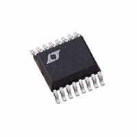
LTC2415-1CGN Linear Technology, LTC2415-1CGN Datasheet - Page 15

LTC2415-1CGN
Manufacturer Part Number
LTC2415-1CGN
Description
IC ADC 24BIT DIFFINPUT/REF16SSOP
Manufacturer
Linear Technology
Datasheet
1.LTC2415CGNPBF.pdf
(40 pages)
Specifications of LTC2415-1CGN
Number Of Bits
24
Sampling Rate (per Second)
13.75
Data Interface
MICROWIRE™, Serial, SPI™
Number Of Converters
2
Power Dissipation (max)
1mW
Voltage Supply Source
Single Supply
Operating Temperature
0°C ~ 70°C
Mounting Type
Surface Mount
Package / Case
16-SSOP (0.150", 3.90mm Width)
Lead Free Status / RoHS Status
Contains lead / RoHS non-compliant
Available stocks
Company
Part Number
Manufacturer
Quantity
Price
Company:
Part Number:
LTC2415-1CGN
Manufacturer:
LT
Quantity:
10 000
Part Number:
LTC2415-1CGN
Manufacturer:
LINEAR/凌特
Quantity:
20 000
Company:
Part Number:
LTC2415-1CGN#PBF
Manufacturer:
TI
Quantity:
120
Part Number:
LTC2415-1CGN#PBF
Manufacturer:
LINEAR/凌特
Quantity:
20 000
Part Number:
LTC2415-1CGN#TRPBF
Manufacturer:
LINEAR/凌特
Quantity:
20 000
APPLICATIO S I FOR ATIO
While the variation in offset with supply voltage is propor-
tional to V
variation can be used to eliminate the effects. First, the
variation with respect to supply voltage is linear. Second,
the magnitude of the offset error decreases with de-
creased supply voltage. Third, the offset error increases
–100
–150
–200
–250
–50
50
0
2.5
V
T
REF
A
Table 2. LTC2415/LTC2415-1 Output Data Format
Differential Input Voltage
V
V
0.5 • V
0.25 • V
0.25 • V
0
–1LSB
– 0.25 • V
– 0.25 • V
– 0.5 • V
V
*The differential input voltage V
= 25 C
Figure 4. Offset vs V
IN
IN
IN
= 2.5V
3.0
CC
* 0.5 • V
* < –0.5 • V
*
SDO
SCK
CS
(see Figure 4), several characteristics of this
REF
REF
REF
REF
3.5
REF
REF
** – 1LSB
**
** – 1LSB
**
Hi-Z
SLEEP
**
** – 1LSB
V
REF
CC
REF
U
4.0
**
(V)
**
PART NO.3
PART NO.2
BIT 31
EOC
4.5
PART NO.1
U
CC
1
5.0
BIT 30
2415 F04
IN
“0”
= IN
5.5
Bit 31
W
EOC
2
0
0
0
0
0
0
0
0
0
0
+
– IN
BIT 29
–103.8
–104.0
–104.2
–104.4
–104.6
–
SIG
.
Bit 30
DMY
3
Figure 5. Offset vs Temperature
–50
0
0
0
0
0
0
0
0
0
0
Figure 3. Output Data Timing
U
BIT 28
MSB
–25
Bit 29
4
DATA OUTPUT
SIG
1
1
1
1
1
0
0
0
0
0
TEMPERATURE ( C)
0
BIT 27
Bit 28
25
MSB
5
with increased reference voltage with an equal and oppo-
site magnitude to the supply voltage variation. As a result,
by tying V
nearly eliminated, see Figure 6. The variation with supply
is less than 2ppm over the entire 2.7V to 5.5V supply
range.
1
0
0
0
0
1
1
1
1
0
**The differential reference voltage V
50
Bit 27
26
0
1
1
0
0
1
1
0
0
1
75
CC
2415 F05
100
LSB
to V
BIT 5
Bit 26
24
LTC2415/LTC2415-1
27
0
1
0
1
0
1
0
1
0
1
REF
–103.0
–103.5
–104.0
–104.5
–105.0
–105.5
, the variation with supply can be
BIT 0
Figure 6. Offset vs V
Bit 25
32
2.7
0
1
0
1
0
1
0
1
0
1
V
V
REF
REF
CC
REF
+
–
3.1
= 5V
REF
= 5V
= 5V
= GND
T
T
CONVERSION
A
T
A
= REF
A
=100 C
=25 C
= –50 C
…
…
…
…
…
…
…
…
…
…
…
3.5
V
IN
IN
F
V
O
IN
CC
+
+
–
2415 F03
= GND
= 0V
= GND
= GND
3.9
– REF
AND V
CC
Bit 0
4.3
REF
0
1
0
1
0
1
0
1
0
1
–
(V
.
(V)
REF
4.7
sn2415 24151fs
= V
15
5.1
CC
2415 F06
)
5.5


