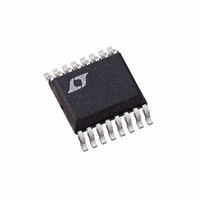
LTC2415-1CGN Linear Technology, LTC2415-1CGN Datasheet - Page 30

LTC2415-1CGN
Manufacturer Part Number
LTC2415-1CGN
Description
IC ADC 24BIT DIFFINPUT/REF16SSOP
Manufacturer
Linear Technology
Datasheet
1.LTC2415CGNPBF.pdf
(40 pages)
Specifications of LTC2415-1CGN
Number Of Bits
24
Sampling Rate (per Second)
13.75
Data Interface
MICROWIRE™, Serial, SPI™
Number Of Converters
2
Power Dissipation (max)
1mW
Voltage Supply Source
Single Supply
Operating Temperature
0°C ~ 70°C
Mounting Type
Surface Mount
Package / Case
16-SSOP (0.150", 3.90mm Width)
Lead Free Status / RoHS Status
Contains lead / RoHS non-compliant
Available stocks
Company
Part Number
Manufacturer
Quantity
Price
Company:
Part Number:
LTC2415-1CGN
Manufacturer:
LT
Quantity:
10 000
Part Number:
LTC2415-1CGN
Manufacturer:
LINEAR/凌特
Quantity:
20 000
Company:
Part Number:
LTC2415-1CGN#PBF
Manufacturer:
TI
Quantity:
120
Part Number:
LTC2415-1CGN#PBF
Manufacturer:
LINEAR/凌特
Quantity:
20 000
Part Number:
LTC2415-1CGN#TRPBF
Manufacturer:
LINEAR/凌特
Quantity:
20 000
LTC2415/LTC2415-1
APPLICATIO S I FOR ATIO
Reference Current
In a similar fashion, the LTC2415/LTC2415-1 sample the
differential reference pins REF
small amount of charge to and from the external driving
circuits thus producing a dynamic reference current. This
current does not change the converter offset, but it may
degrade the gain and INL performance. The effect of this
current can be analyzed in the same two distinct situa-
tions.
For relatively small values of the external reference capaci-
tors (C
settles almost completely and relatively large values for
the source impedance result in only small errors. Such
values for C
gain performance without significant benefits of reference
30
Figure 27. +FS Error vs R
Figure 25. +FS Error vs R
REF
< 0.01 F), the voltage on the sampling capacitor
REF
–180
–270
–360
–450
–10
–20
–30
–40
–50
–90
0
0
will deteriorate the converter offset and
1
0 100 200 300 400 500 600 700 800 900 1000
V
REF
REF
IN
IN
F
T
V
REF
REF
IN
IN
F
T
O
CC
A
U
O
A
CC
+
–
= GND
= 25 C
+
–
+
= 5V
= GND
= 25 C
–
= 2.5V
C
= 5V
+
–
= 3.75V
= 1.25V
10
= 5V
C
REF
= 5V
= GND
C
= 5V
= GND
REF
SOURCE
REF
C
SOURCE
= 0.001 F
REF
= 0.01 F
= 100pF
U
= 0pF
100
R
R
SOURCE
SOURCE
at REF
at REF
+
C
REF
( )
1k
and REF
( )
+
W
C
= 1 F, 10 F
C
+
and REF
REF
REF
or REF
= 0.01 F
10k
= 0.1 F
–
2415 F25
–
2415 F27
–
(Small C
transferring
100k
(Large C
U
IN
REF
)
)
filtering and the user is advised to avoid them.
Larger values of reference capacitors (C
be required as reference filters in certain configurations.
Such capacitors will average the reference sampling charge
and the external source resistance will see a quasi con-
stant reference differential impedance. For the LTC2415,
when F
typical differential reference resistance is 1.3M which
will generate a gain error of approximately 0.38ppm for
each ohm of source resistance driving REF
When F
typical differential reference resistance is 1.56M which
will generate a gain error of approximately 0.32ppm for
each ohm of source resistance driving REF
the LTC2415-1, the typical differential reference resis-
Figure 28. –FS Error vs R
Figure 26. –FS Error vs R
O
O
= LOW (internal oscillator and 60Hz notch), the
= HIGH (internal oscillator and 50Hz notch), the
450
360
270
180
50
40
30
20
10
90
0
0
1
0 100 200 300 400 500 600 700 800 900 1000
V
REF
REF
IN
IN
F
T
V
REF
REF
IN
IN
F
T
O
A
CC
O
CC
A
+
–
+
–
= GND
= 25 C
= GND
= 25 C
+
–
= GND
C
= 5V
= 2.5V
+
–
= 1.25V
= 3.75V
= 5V
C
10
REF
= 5V
= GND
= 5V
= GND
C
REF
REF
SOURCE
C
= 0.001 F
REF
SOURCE
= 0.01 F
= 100pF
= 0pF
R
100
R
SOURCE
SOURCE
at REF
at REF
C
REF
( )
( )
1k
C
REF
= 1 F, 10 F
+
C
+
REF
= 0.01 F
and REF
or REF
10k
= 0.1 F
REF
2415 F26
2415 F28
> 0.01 F) may
+
–
–
100k
or REF
(Small C
(Large C
+
sn2415 24151fs
or REF
–
. For
IN
REF
)
–
)
.


