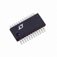
LTC1598LCG Linear Technology, LTC1598LCG Datasheet - Page 11

LTC1598LCG
Manufacturer Part Number
LTC1598LCG
Description
IC A/D CONV 12BIT SRL 8CH 24SSOP
Manufacturer
Linear Technology
Datasheet
1.LTC1598LCGPBF.pdf
(24 pages)
Specifications of LTC1598LCG
Number Of Bits
12
Sampling Rate (per Second)
10.5k
Data Interface
MICROWIRE™, QSPI™, Serial, SPI™
Number Of Converters
1
Power Dissipation (max)
480µW
Voltage Supply Source
Single Supply
Operating Temperature
0°C ~ 70°C
Mounting Type
Surface Mount
Package / Case
24-SSOP (0.200", 5.30mm Width)
Lead Free Status / RoHS Status
Contains lead / RoHS non-compliant
Available stocks
Company
Part Number
Manufacturer
Quantity
Price
Company:
Part Number:
LTC1598LCG
Manufacturer:
LINEAR
Quantity:
320
APPLICATIONS
Data Transfer
The CLK synchronizes the data transfer with each bit
being transmitted on the falling CLK edge and captured
on the rising CLK edge in both transmitting and receiving
systems.
The LTC1594L/LTC1598L first receive input data and
then transmit back the A/D conversion results (half
duplex). Because of the half duplex operation, D
D
just 3 wires: CS, CLK and DATA (D
Data transfer is initiated by a rising chip select (CS)
signal. After CS rises, the input data on the D
latched into a 4-bit register on the rising edge of the clock.
More than four input bits can be sent to the D
without problems, but only the last four bits clocked in
before CS falls will be stored into the 4-bit register. This
4-bit input data word will select the channel in the
muliplexer (see Input Data Word and Tables 1 and 2). To
ensure correct operation, the CS must be pulled low
before the next rising edge of the clock.
Once the CS is pulled low, all channels are simulta-
neously switched off after a delay of t
OUT
may be tied together allowing transmission over
CSMUX = CSADC = CS
COM = GND
MUXOUT
ADCIN =
CH0 TO
D
CH7
CLK
OUT
D
U
IN
INFORMATION
Figure 2. LTC1594L/LTC1598L Operating Sequence Example: All Channels Off
U
EN
D2
Hi-Z
W
IN
D1
/D
D0
OUT
OFF
).
t
to ensure a
OFF
t
suCS
U
IN
NULL
BIT
IN
IN
pin is
and
pin
break-before-make interval, t
(t
allowing the ADC in the chip to acquire input signal and
start the conversion (see Figures 1 and 2). After 1 null bit,
the result of the conversion is output on the D
The selected channel remains on, until the next falling
edge of CS. At the end of the data exchange, CS should
be brought high. This resets the LTC1594L/LTC1598L
and initiates the next data exchange.
Break-Before-Make
The LTC1594L/LTC1598L provide a break-before-make
interval from switching off all the channels simulta-
neously to switching on the next selected channel once
CS is pulled low. In other words, once CS is pulled low,
t
CYC
ADDRESS IN
OFF
SHIFT MUX
D0N‘T CARE
DUMMY CONVERSION
+ t
t
CS
CONV
OPEN
D
t
SMPL
IN1
), the selected channel is switched on,
+ 1 NULL BIT
LTC1594L/LTC1598L
D
OUT1
OPEN
SHIFT A/D CONVERSION
RESULT OUT
. After a delay of t
D
IN2
Hi-Z
1594L/98L F02
D
OUT2
OUT
11
1594L/98L AI01
15948lfb
line.
ON


