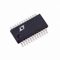
LTC1598LCG Linear Technology, LTC1598LCG Datasheet - Page 20

LTC1598LCG
Manufacturer Part Number
LTC1598LCG
Description
IC A/D CONV 12BIT SRL 8CH 24SSOP
Manufacturer
Linear Technology
Datasheet
1.LTC1598LCGPBF.pdf
(24 pages)
Specifications of LTC1598LCG
Number Of Bits
12
Sampling Rate (per Second)
10.5k
Data Interface
MICROWIRE™, QSPI™, Serial, SPI™
Number Of Converters
1
Power Dissipation (max)
480µW
Voltage Supply Source
Single Supply
Operating Temperature
0°C ~ 70°C
Mounting Type
Surface Mount
Package / Case
24-SSOP (0.200", 5.30mm Width)
Lead Free Status / RoHS Status
Contains lead / RoHS non-compliant
Available stocks
Company
Part Number
Manufacturer
Quantity
Price
Company:
Part Number:
LTC1598LCG
Manufacturer:
LINEAR
Quantity:
320
LTC1594L/LTC1598L
TYPICAL APPLICATIONS
20
START BSET 0,$02 Bit 0 Port C ($02) goes high (CS goes high)
LOOP1 TST $0B
TRANSMIT
RECEIVED
= CSADC
CSMUX
WORD
WORD
D
MPU
MPU
= CS
CLK
OUT
D
LDA #$52
STA $0A
LDA #$FF
STA $04
STA $05
STA $06
LDA #$08
STA $50
LDA $50
STA $0C
IN
#00
#01
0
?
B6
D OUT FROM LTC1598L STORED IN MC68HC05 RAM
0
0
?
Configuration data for serial peripheral
control register (Interrupts disabled, output
enabled, master, Norm = 0, Ph = 0, Clk/16)
Load configuration data into location $0A (SPCR)
Configuration data for I/O ports
(all bits are set as outputs)
Load configuration data into Port A DDR ($04)
Load configuration data into Port B DDR ($05)
Load configuration data into Port C DDR ($06)
Put D
(CH0 with respect to GND)
Load D
Load D
Load D
start clocking data
Test status of SPIF bit in SPI status register ($0B)
0
?
B5
0
IN
IN
IN
IN
word for LTC1598L into Accumulator
0
?
BYTE 1
BYTE 1
word into memory location $50
word at $50 into Accumulator
word into SPI data register ($0C) and
B4
0
EN
EN
?
MSB
B11
B3
D2
D2
?
U
Hardware and Software Interface to Motorola MC68HC05
B10
B2
D1
D1
?
Data Exchange Between LTC1598L and MC68HC05
N
DO
D0
B9
B1
?
LSB
B8
B0
X
?
B7
0
X
?
MC68HC05 CODE
BYTE 1
BYTE 2
X
0
B11
B11 B10 B9
BYTE 2
BYTE 2
X
LOOP2 TST $0B
LOOP3 TST $0B
ANALOG
INPUTS
B10
X
BPL LOOP1 Loop if not done with transfer to previous instruction
BCLR 0,$02 Bit 0 Port C ($02) goes low (CS goes low)
LDA $0C
STA $0C
BPL LOOP2 Loop if not done
LDA $0C
STA $0C
AND #$IF
STA $00
BPL LOOP3 Loop if not done
LDA $0C
AND #$FE
STA $01
JMP START Go back to start and repeat program
B9
X
B8
B8
X
LTC1598L
DON‘T CARE
B7
B7
X
Load contents of SPI data register into Accumulator
Start next SPI cycle
Test status of SPIF
Load contents of SPI data register into Accumulator
Start next SPI cycle
Clear 3 MSBs of first D
Load Port A ($00) with MSBs
Test status of SPIF
Load contents of SPI data register into Accumulator
Clear LSB of second D
Load Port B ($01) with LSBs
CSMUX
CSADC
B6
D
CLK
OUT
D
B6
IN
X
B5
B5
X
B4
B4
X
OUT
OUT
B3
B3
BYTE 3
X
BYTE 3
SCK
MOSI
MISO
C0
word
word
MC68HC05
B2
B2
X
1594L/98L TA04
B1
B1
X
B0
B0
X
1594L/98L TA03
B1
X
B1
15948lfb
B2


