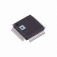
AD9244BST-65 Analog Devices Inc, AD9244BST-65 Datasheet - Page 19

AD9244BST-65
Manufacturer Part Number
AD9244BST-65
Description
IC ADC 14BIT 65MSPS 48-LQFP
Manufacturer
Analog Devices Inc
Datasheet
1.AD9244BSTZ-65.pdf
(36 pages)
Specifications of AD9244BST-65
Rohs Status
RoHS non-compliant
Number Of Bits
14
Sampling Rate (per Second)
65M
Data Interface
Parallel
Number Of Converters
1
Power Dissipation (max)
550mW
Voltage Supply Source
Analog and Digital
Operating Temperature
-40°C ~ 85°C
Mounting Type
Surface Mount
Package / Case
48-LQFP
For Use With
AD9244-65PCBZ - BOARD EVAL FOR AD9244-65AD9244-40PCBZ - BOARD EVAL FOR AD9244-40
Available stocks
Company
Part Number
Manufacturer
Quantity
Price
Company:
Part Number:
AD9244BST-65
Manufacturer:
ADI
Quantity:
624
Part Number:
AD9244BST-65
Manufacturer:
ADI/亚德诺
Quantity:
20 000
The optimum noise and dc linearity performance for either
differential or single-ended inputs is achieved with the largest
input signal voltage span (that is, 2 V input span) and matched
input impedance for VIN+ and VIN–. Only a slight degradation
in dc linearity performance exists between the 2 V and 1 V
input spans; however, the SNR is lower in the 1 V input span.
When the ADC is driven by an op amp and a capacitive load is
switched onto the output of the op amp, the output momentar-
ily drops due to its effective output impedance. As the output
recovers, ringing can occur. To remedy the situation, a series
resistor, R
input, as shown in Figure 45. A shunt capacitance also acts like
a charge reservoir, sinking or sourcing the additional charge
required by the sampling capacitor, C
transients seen at the op amp’s output.
The optimum size of this resistor is dependent on several
factors, including the ADC sampling rate, the selected op amp,
and the particular application. In most applications, a 30 Ω to
100 Ω resistor is sufficient.
For noise-sensitive applications, the very high bandwidth of the
AD9244 can be detrimental, and the addition of a series resistor
and/or shunt capacitor can help limit the wideband noise at the
ADC’s input by forming a low-pass filter. The source impedance
driving VIN+ and VIN− should be matched. Failure to provide
matching can result in degradation of the SNR, THD, and SFDR
performance.
Single-Ended Input Configuration
A single-ended input can provide adequate performance in
cost-sensitive applications. In this configuration, there is
degradation in distortion performance due to large input
common-mode swing. However, if the source impedances on
each input are matched, there should be little effect on SNR
performance.
The internal reference can be used to drive the inputs. Figure 45
shows an example of VREF driving VIN−. In this operating
mode, a 5 Ω resistor and a 0.1 μF capacitor must be connected
between VREF and VIN−, as shown in Figure 45, to limit the
reference noise sampled by the analog input.
S
Figure 45. Resistors Isolating SHA Input from Op Amp
, can be inserted between the op amp and the SHA
+
V
V
CC
EE
10μF
0.1μF
0.1μF
5Ω
20pF
33Ω
33Ω
R
R
C
S
S
S
S
VIN+
VIN–
VREF
SENSE
REFCOM
, further reducing current
AD9244
Rev. C | Page 19 of 36
Differentially Driving the Analog Inputs
The AD9244 has a very flexible input structure, allowing it to
interface with single-ended or differential inputs.
The optimum mode of operation, analog input range, and associ-
ated interface circuitry is determined by the particular application’s
performance requirements as well as power supply options.
Differential operation requires that VIN+ and VIN− be
simultaneously driven with two equal signals that are 180°out of
phase with each other.
Differential modes of operation (ac-coupled or dc-coupled input)
provide the best SFDR performance over a wide frequency range.
They should be considered for the most demanding spectral-
based applications; that is, direct IF conversion to digital.
Because not all applications have a signal precondition for
differential operation, there is often a need to perform a single-
ended-to-differential conversion. In systems that do not require
dc coupling, an RF transformer with a center tap is the best
method for generating differential input signals for the AD9244.
This provides the benefit of operating the ADC in the differen-
tial mode without contributing additional noise or distortion.
An RF transformer also has the added benefit of providing
electrical isolation between the signal source and the ADC.
The differential input characterization was performed using the
configuration in Figure 46. The circuit uses a Mini-Circuits® RF
transformer, model T1-1T, which has an impedance ratio of 1:1.
This circuit assumes that the signal source has a 50 Ω source
impedance. The secondary center tap of the transformer allows
a dc common-mode voltage to be added to the differential input
signal. In Figure 46, the center tap is connected to a resistor
divider providing a half supply voltage. It could also be
connected to the CML pin of the AD9244. For IF sampling
applications (70 MHz < f
the 20 pF differential capacitor between VIN+ and VIN− be
reduced or removed.
MINI-CIRCUITS
50Ω
T1–1T
0.1μF
Figure 46. Transformer-Coupled Input
33Ω
33Ω
R
R
S
S
1kΩ
AVDD
IN
1kΩ
20pF
< 200 MHz), it is recommended that
VIN+
VIN–
AD9244
REFB
REFT
0.1μF
0.1μF
0.1μF
AD9244
+
10μF


