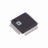
AD9244BST-65 Analog Devices Inc, AD9244BST-65 Datasheet - Page 26

AD9244BST-65
Manufacturer Part Number
AD9244BST-65
Description
IC ADC 14BIT 65MSPS 48-LQFP
Manufacturer
Analog Devices Inc
Datasheet
1.AD9244BSTZ-65.pdf
(36 pages)
Specifications of AD9244BST-65
Rohs Status
RoHS non-compliant
Number Of Bits
14
Sampling Rate (per Second)
65M
Data Interface
Parallel
Number Of Converters
1
Power Dissipation (max)
550mW
Voltage Supply Source
Analog and Digital
Operating Temperature
-40°C ~ 85°C
Mounting Type
Surface Mount
Package / Case
48-LQFP
For Use With
AD9244-65PCBZ - BOARD EVAL FOR AD9244-65AD9244-40PCBZ - BOARD EVAL FOR AD9244-40
Available stocks
Company
Part Number
Manufacturer
Quantity
Price
Company:
Part Number:
AD9244BST-65
Manufacturer:
ADI
Quantity:
624
Part Number:
AD9244BST-65
Manufacturer:
ADI/亚德诺
Quantity:
20 000
AD9244
EVALUATION BOARD
ANALOG INPUT CONFIGURATION
Table 12 provides a summary of the analog input configuration.
The analog inputs of the AD9244 on the evaluation board can
be driven differentially through a transformer via Connector S4,
or through the
be driven single-ended directly via Connector S3. When using
the transformer or
be used, as both of these devices are configured on the AD9244
evaluation board to convert single-ended signals to differential
signels.
Optimal AD9244 performance is achieved above 500 kHz by
using the input transformer. To drive the AD9244 via the trans-
former, connect solderable Jumper JP45 and Jumper JP46. DC
bias is provided by Resistor R8 and Resistor R28. The evaluation
board has positions for through-hole and surface-mount
transformers.
For applications requiring lower frequencies or dc applications,
the
and noise performance, as well as input buffering up to 30 MHz.
For more information, refer to the
the
or T4) and connect solderable Jumper JP42 and Jumper JP43.
The AD9244 can be driven single-ended directly via S3 and can
be ac-coupled or dc-coupled by removing or inserting JP5. To
run the evaluation board in this way, remove the transformer
(T1 or T4) and connect solderable Jumper JP40 and Jumper JP41.
Resistor R40, Resistor R41, Resistor R8, and Resistor R28 are
used to bias the AD9244 inputs to the correct common-mode
levels in this application.
Table 12. Analog Input Jumper Configuration
Analog Input
Differential: Transformer
Differential: Amplifier
Single-Ended
Table 13. Reference Jumper Configuration
Reference
Internal
Internal
Internal
External
AD8138
AD8138
can be used. The
to drive the AD9244, remove the transformer (T1
AD8138
AD8138
Voltage
2 V
1 V
1 V ≤ VREF ≤ 2 V
1 V ≤ VREF ≤ 2 V
amplifier via Connector S2, or they can
Input Connector
S4
S2
S3
amplifier, a single-ended source can
AD8138
AD8138
provides good distortion
data sheet. To use
Jumpers
45, 46
42, 43
5, 40, 41
Jumpers
23
24
25
8, 22
Notes
R8, R28 provide dc bias; optimal for 500 kHz.
Remove T1 or T4; used for low input frequencies.
Remove T1 or T4. JP5: connected for dc-coupled, not connected for ac-coupling.
Rev. C | Page 26 of 36
REFERENCE CONFIGURATION
As described in the Analog Input and Reference Overview
section, the AD9244 can be configured to use its own internal
or an external reference. An external reference, D3, and refer-
ence buffer, U5, are included on the AD9244 evaluation board.
Jumper JP8 and Jumper JP22 to Jumper JP24 can be used to
select the desired reference configuration (see Table 13).
CLOCK CONFIGURATION
The AD9244 evaluation board was designed to achieve optimal
performance as well as to be easily configurable by the user. To
configure the clock input, begin by connecting the correct com-
bination of solderable jumpers (see Table 14). The specific
jumper configuration is dependent on the application and can
be determined by referring to the Clock Input Modes section. If
the differential clock input mode is selected, an external sine
wave generator applied to S5 can be used as the clock source.
The clock buffer/drive MC10EL16 from ON Semiconductor® is
used on the evaluation board to buffer and square the clock
input. If the single-ended clock configuration is used, an exter-
nal clock source can be applied to S1.
The AD9244 evaluation board generates a buffered clock at
TTL/CMOS levels for use with a data capture system, such as
the HSC-ADC-EVAL-SC system. The clock buffering is pro-
vided by U4 and U7 and is configured by Jumper JP3,
Jumper JP4, Jumper JP9, and Jumper JP18 (see Table 14).
Notes
JP8 not connected
JP8 not connected
JP8 not connected; VREF = 1 + R1/R2
Set VREF with R26


