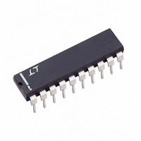
LTC1090CN#PBF Linear Technology, LTC1090CN#PBF Datasheet - Page 16

LTC1090CN#PBF
Manufacturer Part Number
LTC1090CN#PBF
Description
IC DATA ACQUIS SYS 10BIT 20-DIP
Manufacturer
Linear Technology
Type
Data Acquisition System (DAS), ADCr
Datasheet
1.LTC1090CNPBF.pdf
(28 pages)
Specifications of LTC1090CN#PBF
Resolution (bits)
10 b
Sampling Rate (per Second)
30k
Data Interface
Serial
Voltage Supply Source
Dual ±
Voltage - Supply
5V
Operating Temperature
-40°C ~ 85°C
Mounting Type
Through Hole
Package / Case
20-DIP (0.300", 7.62mm)
Number Of Elements
1
Resolution
10Bit
Architecture
SAR
Sample Rate
30KSPS
Input Polarity
Unipolar/Bipolar
Input Type
Voltage
Rated Input Volt
5/±5V
Differential Input
Yes
Power Supply Requirement
Single/Dual
Single Supply Voltage (typ)
5V
Single Supply Voltage (min)
4.5V
Single Supply Voltage (max)
10V
Dual Supply Voltage (typ)
±5V
Dual Supply Voltage (min)
0/4.5V
Dual Supply Voltage (max)
-5.5/10V
Power Dissipation
500mW
Differential Linearity Error
1LSB(Typ)
Integral Nonlinearity Error
±0.5LSB
Operating Temp Range
-40C to 85C
Operating Temperature Classification
Industrial
Mounting
Through Hole
Pin Count
20
Package Type
PDIP N
Lead Free Status / RoHS Status
Lead free / RoHS Compliant
Available stocks
Company
Part Number
Manufacturer
Quantity
Price
APPLICATIO S I FOR ATIO
Motorola SPI (MC68HC05C4)
The MC68HC05C4 transfers data MSB first and in 8-bit
increments. Programming the LTC1090 for MSB first
format and 16-bit word length allows the 10-bit data
output to be received by the MPU as two 8-bit bytes with
the final 6 unused bits filled with zeroes by the LTC1090.
LTC1090
16
MNEMONIC
BCLR n
LDA
STA
↑
NOP
↓
LDA
LDA
STA
STA
↑
NOP
↓
BSET n
LDA
LDA
STA
D
Location A
Location A + 1
*B9 is MSB in unipolar or sign bit in bipolar
OUT
Hardware and Software Interface to Motorola MC68HC05C4
Processor
from LTC1090 stored in MC68HCO5C4 RAM
ANALOG
INPUTS
C0 is cleared (CS goes Low)
Load D
Load D
8 NOPs for timing
Load contents of SPI status reg. into ACC
Load LTC1090 D
Load LTC1090 D
Start next SPl cycle
6 NOPs for timing
C0 is set (CS goes high)
Load contents of SPI status reg. into ACC
Load LTC1090 D
Load LTC1090 D
IN
IN
MSB*
B9
B1 B0
LTC1090
U
for LTC1090 into ACC
from ACC to SPI data reg. Start SCK
LSB
SCLK
D
B8 B7 B6 B5 B4 B3 B2
OUT
D
CS
IN
OUT
OUT
OUT
OUT
U
0
from SPI data reg. into ACC (byte 1)
into RAM (location A)
from SPI data reg. into ACC (byte 2)
into RAM (location A + 1)
DESCRIPTION
0
MC68HCO5C4
0
W
CO
SCK
MOSI
MISO
0
0
0
U
LTC1090 • AI12
byte 1
byte 2
Hitachi Synchronous SCI (HD63705)
The HD63705 transfers serial data in 8-bit increments,
LSB first. To accommodate this, the LTC1090 is
programmed for 16-bit word length and LSB first format.
The 10-bit output data is received by the processor as two
8-bit bytes, LSB first. The LTC1090 fills the final 6 unused
bits (after the MSB) with zeroes in unipolar mode and with
the sign bit in bipolar mode.
Hardware and Software Interface to Hitachi HD63705 Processor
MNEMONIC
LDA
BCLR n
STA
↑
NOP
↓
LDA
STA
NOP
BSET n
LDA
STA
Location A
Location A + 1
Location A
Location A + 1
D
OUT
ANALOG
from LTC1090 stored in HD63705 RAM
INPUTS
Load D
C0 cleared (CS goes low)
Load D
and start clocking data (LSB first)
6 NOPs for timing
Load contents of SCI data reg. into ACC (byte 1)
Start next SCI cycle
Load LTC1090 D
Timing
C0 set (CS goes high)
Load contents of SCI data reg. into ACC (byte 2)
Load LTC1090 D
IN
IN
Sign
B9 B9 B9 B9 B9 B9 B9 B8
LTC1090
B7
B7
word for LTC1090 into ACC from RAM
word for LTC1090 into SCI data reg. from ACC
0
SCLK
D
B6 B5 B4 B3 B2 B1 B0
B6 B5 B4 B3 B2 B1 B0
OUT
D
CS
0 0 0 0 0 B9 B8
IN
OUT
OUT
DESCRIPTION
word into RAM (Location A)
word into RAM (Location A + 1)
Bipolar
Unipolar
C0
CK
T
R
HD63705
X
X
MSB
LSB
LSB
LTC1090 • AI13
byte 1
byte 2
byte 1
byte 2
1090fc


