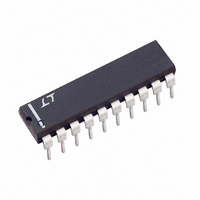
LTC1090CN#PBF Linear Technology, LTC1090CN#PBF Datasheet - Page 19

LTC1090CN#PBF
Manufacturer Part Number
LTC1090CN#PBF
Description
IC DATA ACQUIS SYS 10BIT 20-DIP
Manufacturer
Linear Technology
Type
Data Acquisition System (DAS), ADCr
Datasheet
1.LTC1090CNPBF.pdf
(28 pages)
Specifications of LTC1090CN#PBF
Resolution (bits)
10 b
Sampling Rate (per Second)
30k
Data Interface
Serial
Voltage Supply Source
Dual ±
Voltage - Supply
5V
Operating Temperature
-40°C ~ 85°C
Mounting Type
Through Hole
Package / Case
20-DIP (0.300", 7.62mm)
Number Of Elements
1
Resolution
10Bit
Architecture
SAR
Sample Rate
30KSPS
Input Polarity
Unipolar/Bipolar
Input Type
Voltage
Rated Input Volt
5/±5V
Differential Input
Yes
Power Supply Requirement
Single/Dual
Single Supply Voltage (typ)
5V
Single Supply Voltage (min)
4.5V
Single Supply Voltage (max)
10V
Dual Supply Voltage (typ)
±5V
Dual Supply Voltage (min)
0/4.5V
Dual Supply Voltage (max)
-5.5/10V
Power Dissipation
500mW
Differential Linearity Error
1LSB(Typ)
Integral Nonlinearity Error
±0.5LSB
Operating Temp Range
-40C to 85C
Operating Temperature Classification
Industrial
Mounting
Through Hole
Pin Count
20
Package Type
PDIP N
Lead Free Status / RoHS Status
Lead free / RoHS Compliant
Available stocks
Company
Part Number
Manufacturer
Quantity
Price
APPLICATIO S I FOR ATIO
3. Analog Inputs
Because of the capacitive redistribution A/D conversion
techniques used, the analog inputs of the LTC1090 have
capacitive switching input current spikes. These current
spikes settle quickly and do not cause a problem.
However, if large source resistances are used or if slow
settling op amps drive the inputs, care must be taken to
insure that the transients caused by the current spikes
settle completely before the conversion begins.
Source Resistance
The analog inputs of the LTC1090 look like a 60pF capaci-
tor (C
Figure 9. C
“–” inputs once during each conversion cycle. Large
external source resistors and capacitances will slow the
settling of the inputs. It is important that the overall RC
time constants be short enough to allow the analog inputs
to completely settle within the allowed time.
V
V
IN
IN
+
–
IN
“ + ” INPUT
“ – ” INPUT
) in series with a 500Ω resistor (R
R
R
SOURCE
SOURCE
SCLK
ACLK
IN
CS
Figure 9. Analog Input Equivalent Circuit
gets switched between the selected “+” and
+
–
C1
C2
INPUT
INPUT
U
1
“
“
+
–
”
”
U
MUX ADDRESS
2
SHIFTED IN
4TH SCLK
LAST SCLK
3
W
R
ON
LTC1090
Figure 10. “+” and “–” Input Settling Windows
= 500Ω
SAMPLE
ON
4
) as shown in
SETTLE DURING THIS TIME
U
C
IN
“ + ” INPUT MUST
= 60pF
LTC1090 • AI16
t
SMPL
“+” Input Settling
This input capacitor is switched onto the “+” input during
the sample phase (t
phase starts at the 4th SCLK cycle and lasts until the falling
edge of the last SCLK (the 8th, 10th, 12th or 16th SCLK
cycle depending on the selected word length). The voltage
on the “+” input must settle completely within this sample
time. Minimizing R
settling time. If large “+” input source resistance must be
used, the sample time can be increased by using a slower
SCLK frequency or selecting a longer word length. With
the minimum possible sample time of 4µs, R
and C1 < 20pF will provide adequate settling.
“–” Input Settling
At the end of the sample phase the input capacitor switches
to the “–” input and the conversion starts (see Figure 10).
During the conversion, the “+” input voltage is effectively
“held” by the sample and hold and will not affect the
conversion result. However, it is critical that the “–” input
voltage be free of noise and settle completely during the
first four ACLK cycles of the conversion time. Minimizing
R
“–” input source resistance must be used, the time allowed
for settling can be extended by using a slower ACLK
frequency. At the maximum ACLK rate of 2MHz, R
< 1kΩ and C2 < 20pF will provide adequate settling.
SOURCE
HOLD
“ – ” INPUT MUST SETTLE
DURING THIS TIME
1
LAST SCLK (8TH, 10TH, 12TH OR 16TH DEPENDING ON WORK LENGTH)
–
1ST BIT
TEST
2
and C2 will improve settling time. If large
3
4
SOURCE
SMPL
+
, see Figure 10). The sample
and C1 will improve the input
LTC1090
LTC1090 • AI17
SOURCE
SOURCE
19
+
< 2k
1090fc
–


