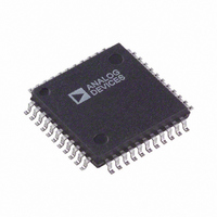
AD2S1200YSTZ Analog Devices Inc, AD2S1200YSTZ Datasheet - Page 18

AD2S1200YSTZ
Manufacturer Part Number
AD2S1200YSTZ
Description
IC CONV R/D 12-BIT W/OSC 44-LQFP
Manufacturer
Analog Devices Inc
Type
R/D Converterr
Datasheet
1.AD2S1200.pdf
(24 pages)
Specifications of AD2S1200YSTZ
Resolution (bits)
12 b
Data Interface
Serial, Parallel
Voltage Supply Source
Analog and Digital
Voltage - Supply
4.75 V ~ 5.25 V
Operating Temperature
-40°C ~ 125°C
Mounting Type
Surface Mount
Package / Case
44-LQFP
Input Channel Type
Differential
Supply Voltage Range - Analog
4.75V To 5.25V
Supply Voltage Range - Digital
4.75V To 5.25V
Lead Free Status / RoHS Status
Lead free / RoHS Compliant
For Use With
EVAL-AD2S1200CBZ - BOARD EVAL FOR AD2S1200
Sampling Rate (per Second)
-
Lead Free Status / RoHS Status
Lead free / RoHS Compliant, Lead free / RoHS Compliant
Available stocks
Company
Part Number
Manufacturer
Quantity
Price
Company:
Part Number:
AD2S1200YSTZ
Manufacturer:
Analog Devices Inc
Quantity:
10 000
AD2S1200
CIRCUIT DYNAMICS
AD2S1200 LOOP RESPONSE MODEL
The RDC is a mixed-signal device, which uses two A/D
converters to digitize signals from the resolver and a Type II
tracking loop to convert these to digital position and velocity
words.
The first gain stage consists of the ADC gain on the Sin/Cos
inputs, and the gain of the error signal into the first integrator.
The first integrator generates a signal proportional to velocity.
The compensation filter contains a pole and a zero, used to
provide phase margin and reduce high frequency noise gain.
The second integrator is the same as the first integrator and
generates the output position from the velocity signal. The
Sin/Cos lookup has unity gain. Values are given below for each
section:
• ADC gain parameter
• Error gain parameter
• Compensator zero coefficient
• Compensator pole coefficient
• Integrator gain parameter
• INT1 and INT2 transfer function
• Compensation filter transfer
• R2D open-loop transfer function
• R2D closed-loop transfer function
θ
IN
(k1
function
nom
–
= 1.8/2.5)
Figure 11. RDC System Response Block Diagram
k1 × k2
(ACCELERATION)
ERROR
1–z
Sin/Cos LOOKUP
c
–1
VELOCITY
1–bz
1–az
k
k
a
b
c
C
G
H
I
–1
–1
1
(
2
=
(
=
(
=
z
(
z
=
z
=
z
)
4096000
)
)
4096
4095
4096
4085
)
=
V
V
18
=
=
=
IN
REF
1
1
1
k
1
1–z
x
1
−
1
(
−
−
10
c
V
c
(
×
+
G
z
V
az
bz
–1
p
−
k
G
(
6
1
)
)
z
2
−
−
(
×
)
1
1
z
×
2
)
I
π
(
z
)
θ
2
OUT
Rev. 0 | Page 18 of 24
×
C
(
z
)
The closed-loop magnitude and phase responses are that of a
second-order low-pass filter (see Figure 12 and Figure 13).
To convert G(z) into the s-plane, we perform an inverse bilinear
transformation by substituting for z, where T = the sampling
period (1/4.096 MHz ≈ 244 ns).
Substitution yields the open-loop transfer function G(s).
This transformation produces the best matching at low
frequencies (f << f
closed-loop bandwidth of the AD2S1200), the transfer function
can be simplified to
where:
Solving for each value gives t
10
By converting to the s-domain, we are able to quantify the
open-loop dc gain (K
of acceleration error of the loop as discussed in the Sources of
Error section.
The step response to a 10° input step is shown in Figure 14.
Because the error calculation (Equation 3) is nonlinear for large
values of θ − ϕ, the response time for larger step changes in
position (90° – 180°) will typically take three times as long as the
response to a small step change in position (<20°). In response
to a step change in velocity, the AD2S1200 will exhibit the same
response characteristics as for a step change in position.
6
s
-
2
. Note that the closed-loop response is described as
G
(
s
)
=
k
1
×
a
k
SAMPLE
2
−
1 (
G
b
a
−
). This value is useful during calculation
(
t
t
K
1
2
s
H
a
). At lower frequencies (within the
a
)
=
)
=
(
×
=
≅
s
T
2
T
z
2
)
1
1 (
1 (
k
1 (
1 (
1
=
=
+
K
1
s
= 1 µs, t
−
+
−
+
×
sT
1
T
T
2
2
2
a
a
a
b
a
+
b
k
G
s
+
−
×
)
)
)
+
)
2
−
2
G
(
1 (
s
s
s
1
s
1
b
(
)
2
s
−
2
T
4
+
+
)
= 90 µs, and K
a
2
st
st
)
×
1
2
1
1
+
+
s
s
×
×
T
T
2
2
1 (
1 (
1 (
1 (
a
−
−
+
+
≈ 7.4 ×
a
b
a
b
)
)
)
)


