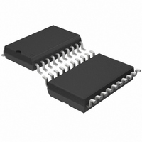
LTC1090CSW Linear Technology, LTC1090CSW Datasheet - Page 6

LTC1090CSW
Manufacturer Part Number
LTC1090CSW
Description
IC DATA ACQUIS SYS 10BIT 20-SOIC
Manufacturer
Linear Technology
Type
Data Acquisition System (DAS), ADCr
Datasheet
1.LTC1090CNPBF.pdf
(28 pages)
Specifications of LTC1090CSW
Resolution (bits)
10 b
Sampling Rate (per Second)
30k
Data Interface
Serial
Voltage Supply Source
Dual ±
Voltage - Supply
5V
Operating Temperature
-40°C ~ 85°C
Mounting Type
Surface Mount
Package / Case
20-SOIC (7.5mm Width)
Lead Free Status / RoHS Status
Contains lead / RoHS non-compliant
Available stocks
Company
Part Number
Manufacturer
Quantity
Price
Part Number:
LTC1090CSW
Manufacturer:
LINEAR/凌特
Quantity:
20 000
Company:
Part Number:
LTC1090CSW#PBF
Manufacturer:
LT
Quantity:
252
Part Number:
LTC1090CSW#TRPBF
Manufacturer:
LINEAR/凌特
Quantity:
20 000
PI FU CTIO S
BLOCK DIAGRA
LTC1090
6
#
1-8
9
10
11
12
13,14
15
16
17
18
19
20
U
PIN
CH0 to CH7
COM
DGND
AGND
V
REF
CS
D
D
SCLK
ACLK
V
U
OUT
IN
CC
–
–
, REF
+
COM
CH0
CH1
CH2
CH3
CH4
CH5
CH6
CH7
V
D
CC
IN
U
FUNCTION
Analog Inputs
Common
Digital Ground
Analog Ground
Negative Supply
Reference Inputs
Chip Select Input
Digital Data Output
Data Input
Shift Clock
A/D Conversion Clock
Positive Supply
20
17
DGND
1
2
3
4
5
6
7
8
9
W
10
INPUT SHIFT
REGISTER
ANALOG
INPUT
MUX
AGND
11
AND HOLD
SAMPLE
DESCRIPTION
The analog inputs must be free of noise with respect to AGND.
The common pin defines the zero reference point for all single ended inputs. It must be free
of noise and is usually tied to the analog ground plane.
This is the ground for the internal logic. Tie to the ground plane.
AGND should be tied directly to the analog ground plane.
Tie V
The reference inputs must be kept free of noise with respect to AGND.
A logic low on this input enables data transfer.
The A/D conversion result is shifted out of this output.
The A/D configuration word is shifted into this input.
This clock synchronizes the serial data transfer.
This clock controls the A/D conversion process.
This supply must be kept free of noise and ripple by bypassing directly to the analog ground
plane.
–
to most negative potential in the circuit. (Ground in single supply applications.)
V –
12
COMP
CAPACITIVE
REF –
10-BIT
DAC
13
REF +
14
REGISTER
CONTROL
OUTPUT
TIMING
10-BIT
SHIFT
SAR
AND
18
16
19
15
SCLK
D
ACLK
CS
LTC1090 • BD01
OUT
1090fc


