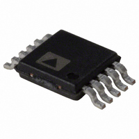
AD5258BRMZ1 Analog Devices Inc, AD5258BRMZ1 Datasheet - Page 16

AD5258BRMZ1
Manufacturer Part Number
AD5258BRMZ1
Description
IC POT DGTL I2C1K 64P 10MSOP
Manufacturer
Analog Devices Inc
Specifications of AD5258BRMZ1
Memory Type
Non-Volatile
Temperature Coefficient
200 ppm/°C Typical
Taps
64
Resistance (ohms)
1K
Number Of Circuits
1
Interface
I²C, 2-Wire Serial
Voltage - Supply
2.7 V ~ 5.5 V
Operating Temperature
-40°C ~ 85°C
Mounting Type
Surface Mount
Package / Case
10-MSOP, Micro10™, 10-uMAX, 10-uSOP
Resistance In Ohms
1.00K
End To End Resistance
1kohm
Resistance Tolerance
± 30%
No. Of Steps
64
Supply Voltage Range
2.7V To 5.5V
No. Of Pots
Single
Control Interface
I2C
Rohs Compliant
Yes
Lead Free Status / RoHS Status
Lead free / RoHS Compliant
For Use With
AD5258EVAL - BOARD EVAL FOR AD5258 DGTL POT
Lead Free Status / RoHS Status
Lead free / RoHS Compliant, Lead free / RoHS Compliant
Available stocks
Company
Part Number
Manufacturer
Quantity
Price
Part Number:
AD5258BRMZ1
Manufacturer:
ADI/亚德诺
Quantity:
20 000
Part Number:
AD5258BRMZ1-R7
Manufacturer:
ADI/亚德诺
Quantity:
20 000
Company:
Part Number:
AD5258BRMZ10
Manufacturer:
ADI
Quantity:
835
Company:
Part Number:
AD5258BRMZ10
Manufacturer:
AD
Quantity:
2 444
Part Number:
AD5258BRMZ10
Manufacturer:
ADI/亚德诺
Quantity:
20 000
Part Number:
AD5258BRMZ10-R7
Manufacturer:
ADI/亚德诺
Quantity:
20 000
Part Number:
AD5258BRMZ100
Manufacturer:
ADI/亚德诺
Quantity:
20 000
AD5258
I
The following generic, write, read, and store/restore control
registers for the AD5258 all refer to the device addresses listed
in Table 5, and the mode/condition reference key (S, P, SA, MA,
NA, W , R, and X) listed below.
S = Start Condition
P = Stop Condition
SA = Slave Acknowledge
MA = Master Acknowledge
NA = No Acknowledge
W = Write
R = Read
X = Don’t Care
GENERIC INTERFACE
Table 6. Generic Interface Format
Table 7. RDAC-to-EEPROM Interface Command Descriptions
C2
0
0
0
1
1
1
S
2
C BYTE FORMATS
7-Bit Device Address
(See Table 5)
Slave Address Byte
C1
0
0
1
0
0
1
C0
0
1
0
0
1
0
R/W SA C2 C1 C0 A4 A3 A2 A1 A0 SA D7 D6 D5 D4 D3 D2 D1 D0 SA P
Command Description
Operation between I
Operation between I
Operation between I
Register. See Table 10.
NOP
Restore EEPROM to RDAC
Store RDAC to EEPROM
Instruction Byte
2
2
2
C and RDAC
C and EEPROM
C and Write Protection
Rev. 0 | Page 16 of 24
Table 5. Device Address Lookup
AD1 and AD0 are three-state address pins.
Device Address
0011000
0011001
0011010
0101001
0101010
0101011
1001100
1001101
1001110
Data Byte
AD1
0
NC
1
0
NC
1
0
NC
1
0
AD0
0
0
NC
NC
NC
1
1
1


