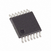
DS1855E-050+ Maxim Integrated Products, DS1855E-050+ Datasheet - Page 6

DS1855E-050+
Manufacturer Part Number
DS1855E-050+
Description
IC RES TEMP-CNTRL 10/50K 14TSSOP
Manufacturer
Maxim Integrated Products
Datasheet
1.DS1855E-010.pdf
(20 pages)
Specifications of DS1855E-050+
Taps
100, 256
Resistance (ohms)
10K, 50K
Number Of Circuits
2
Temperature Coefficient
750 ppm/°C Typical
Memory Type
Non-Volatile
Interface
I²C, 2-Wire Serial
Voltage - Supply
2.7 V ~ 5.5 V
Operating Temperature
-40°C ~ 85°C
Mounting Type
Surface Mount
Package / Case
14-TSSOP
Resistance In Ohms
10K and 50K
Lead Free Status / RoHS Status
Lead free / RoHS Compliant
DS1855
2-WIRE OPERATION
Clock and Data Transitions
The SDA pin is normally pulled high with an external resistor or device. Data on the SDA pin may only
change during SCL low time periods. Data changes during SCL high periods will indicate a START or
STOP conditions depending on the conditions discussed below. Refer to the timing diagram in Figure 2
for further details.
START Condition
A high-to-low transition of SDA with SCL high is a START condition that must precede any other
command. Refer to the timing diagram in Figure 2 for further details.
STOP Condition
A low-to-high transition of SDA with SCL high is a STOP condition. After a read sequence, the stop
command places the DS1855 into a low-power mode. Refer to the timing diagram in Figure 2 for further
details.
Acknowledge
All address and data bytes are transmitted via a serial protocol. The DS1855 pulls the SDA line low
during the ninth clock pulse to acknowledge that it has received each word.
Standby Mode
The DS1855 features a low-power mode that is automatically enabled after power-on, after a STOP
command, and after the completion of all internal operations.
2-Wire Interface Reset
After any interruption in protocol, power loss, or system reset, the following steps reset the DS1855:
1. Clock up to nine cycles.
2. Look for SDA high in each cycle while SCL is high.
3. Create a START condition while SDA is high.
Device Addressing
The DS1855 must receive an 8-bit device address word following a START condition to enable a specific
device for a read or write operation. The address word is clocked into the DS1855 MSB to LSB. The
address word consists of Ah (1010) followed by A2, A1, and A0 then the read/write (R/W) bit. If the
R/W bit is high, a read operation is initiated. If the R/W is low, a write operation is initiated. For a device
to become active, the values of A2, A1, and A0 must be the same as the hard-wired address pins on the
DS1855. Upon a match of written and hard-wired addresses, the DS1855 will output a zero for one clock
cycle as an acknowledge. If the address does not match, the DS1855 returns to a low-power mode.
Write Operations
After receiving a matching address byte with the R/W bit set low, the device goes into the write mode of
operation. The master must transmit an 8-bit EEPROM memory address to the device to define the
address where the data is to be written. After the reception of this byte, the DS1855 will transmit a zero
for one clock cycle to acknowledge the receipt of the address. The master must then transmit an 8-bit data
word to be written into this address. The DS1855 will again transmit a zero for one clock cycle to
acknowledge the receipt of the data. At this point, the master must terminate the write operation with a
STOP condition. The DS1855 then enters an internally timed write process T
to the EEPROM memory.
w
All inputs are disabled during this byte write cycle.
6 of 6


