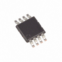
MAX5304CUA+ Maxim Integrated Products, MAX5304CUA+ Datasheet - Page 9

MAX5304CUA+
Manufacturer Part Number
MAX5304CUA+
Description
IC DAC 10BIT LP VOLT OUT 8-UMAX
Manufacturer
Maxim Integrated Products
Datasheet
1.MAX5304CUA.pdf
(12 pages)
Specifications of MAX5304CUA+
Settling Time
10µs
Number Of Bits
10
Data Interface
Serial
Number Of Converters
1
Voltage Supply Source
Single Supply
Operating Temperature
0°C ~ 70°C
Mounting Type
Surface Mount
Package / Case
8-MSOP, Micro8™, 8-uMAX, 8-uSOP,
Number Of Dac Outputs
1
Resolution
10 bit
Interface Type
Serial (SPI)
Supply Voltage (max)
5.5 V
Supply Voltage (min)
4.5 V
Maximum Operating Temperature
+ 70 C
Mounting Style
SMD/SMT
Minimum Operating Temperature
0 C
Supply Current
400 uA
Voltage Reference
External
Lead Free Status / RoHS Status
Lead free / RoHS Compliant
Power Dissipation (max)
-
Lead Free Status / Rohs Status
Lead free / RoHS Compliant
Figure 7 shows a method of connecting several
MAX5304s. In this configuration, the clock and the data
bus are common to all devices, and separate chip-
select lines are used for each IC.
For a unipolar output, the output voltage and the refer-
ence input have the same polarity. Figure 8 shows the
MAX5304 unipolar output circuit, which is also the typi-
cal operating circuit. Table 2 lists the unipolar output
codes.
Figure 9 illustrates a Rail-to-Rail
This circuit shows the MAX5304 with the output amplifi-
er configured for a closed-loop gain of +2V/V to provide
a 0 to 5V full-scale range when a 2.5V reference is used.
The MAX5304 output can be configured for bipolar
operation using Figure 10’s circuit according to the fol-
lowing equation:
where NB is the numeric value of the DAC’s binary
input code. Table 3 shows digital codes (offset binary)
and corresponding output voltages for Figure 10’s cir-
cuit.
Figure 7. Multiple MAX5304s Sharing Common DIN and SCLK Lines
Rail-to-Rail is a registered trademark of Nippon Motorola, Ltd.
SCLK
CS1
CS2
CS3
DIN
V
OUT
Applications Information
= V
_______________________________________________________________________________________
REF
[(2NB / 1024) - 1]
CS
SCLK
DIN
MAX5304
®
output configuration.
Unipolar Output
Bipolar Output
10-Bit Voltage-Output DAC
CS
SCLK
DIN
MAX5304
In applications where the reference has AC signal com-
ponents, the MAX5304 has multiplying capability within
the reference input range specifications. Figure 11
shows a technique for applying a sine-wave signal to
the reference input where the AC signal is offset before
being applied to REF. The reference voltage must
never be more negative than GND.
Table 2. Unipolar Output Codes
Note: ( ) are for sub-bits.
MSB
1 1 1 1 1 1 1 1 1 1 ( 0 0 0 )
1 0 0 0 0 0 0 0 0 1 ( 0 0 0 )
1 0 0 0 0 0 0 0 0 0 ( 0 0 0 )
0 1 1 1 1 1 1 1 1 1 ( 0 0 0 )
0 0 0 0 0 0 0 0 0 1 ( 0 0 0 )
0 0 0 0 0 0 0 0 0 0 ( 0 0 0 )
DAC CONTENTS
CS
SCLK
DIN
LSB
in 8-Pin µMAX
MAX5304
Using an AC Reference
+V
REF
ANALOG OUTPUT
+V
+V
+V
+V
REF
REF
1024
REF
REF
512
TO OTHER
SERIAL DEVICES
0V
=
1024
1024
1024
1024
1023
513
511
1
+
V
REF
2
9


