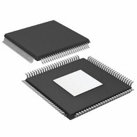
AD9785BSVZ Analog Devices Inc, AD9785BSVZ Datasheet - Page 50

AD9785BSVZ
Manufacturer Part Number
AD9785BSVZ
Description
IC DAC 12BIT 800MSPS 100TQFP
Manufacturer
Analog Devices Inc
Series
TxDAC®r
Datasheet
1.AD9785BSVZ.pdf
(64 pages)
Specifications of AD9785BSVZ
Data Interface
Serial
Number Of Bits
12
Number Of Converters
2
Voltage Supply Source
Analog and Digital
Power Dissipation (max)
450mW
Operating Temperature
-40°C ~ 85°C
Mounting Type
Surface Mount
Package / Case
100-TQFP Exposed Pad, 100-eTQFP, 100-HTQFP, 100-VQFP
Resolution (bits)
12bit
Sampling Rate
800MSPS
Input Channel Type
Parallel
Digital Ic Case Style
QFP
No. Of Pins
100
Operating Temperature Range
-40°C To +85°C
Lead Free Status / RoHS Status
Lead free / RoHS Compliant
Settling Time
-
Lead Free Status / RoHS Status
Lead free / RoHS Compliant, Lead free / RoHS Compliant
Available stocks
Company
Part Number
Manufacturer
Quantity
Price
Company:
Part Number:
AD9785BSVZ
Manufacturer:
Analog Devices Inc
Quantity:
135
Company:
Part Number:
AD9785BSVZ
Manufacturer:
Analog Devices Inc
Quantity:
10 000
Company:
Part Number:
AD9785BSVZRL
Manufacturer:
Analog Devices Inc
Quantity:
10 000
AD9785/AD9787/AD9788
ANALOG OUTPUTS
Full-scale current on the I DAC and Q DAC can be set from
8.66 mA to 31.66 mA. Initially, the 1.2 V band gap reference is
used to set up a current in an external resistor connected to
I120 (Pin 75). A simplified block diagram of the reference
circuitry is shown in Figure 69.
The recommended value for the external resistor is 10 kΩ,
which sets up an I
turn provides a DAC output full-scale current of 20 mA. Because
the gain error is a linear function of this resistor, a high precision
resistor improves gain matching to the internal matching
specification of the devices. Internal current mirrors provide
a current-gain scaling, where DAC gain is a 10-bit word in the
SPI port register (Register 0x05 and Register 0x07). The default
value for the DAC gain registers gives an I
20 mA, where I
0.1µF
1
.
2
R
35
30
25
20
15
10
VREF
V
5
0
10kΩ
I120
0
Figure 70. DAC Full-Scale Current vs. DAC Gain Code
Figure 69. Full-Scale Current Generation Circuitry
12
27
FS
for either I DAC or Q DAC is equal to
REFERENCE
5kΩ
200
1.2V BAND GAP
REFERENCE
1024
AD9788
6
in the resistor of 120 μA, which in
DAC GAIN CODE
DAC gain
400
Q DAC GAIN
I DAC GAIN
CURRENT
SCALING
600
FS
32
of approximately
Q DAC
I DAC
800
DAC FULL-SCALE
REFERENCE
CURRENT
1000
Rev. A | Page 50 of 64
DIGITAL AMPLITUDE SCALING
Gain scaling of the analog DAC output can be achieved by
changing the values in Register 0x05 and Register 0x07.
However, if this is done, the output common-mode voltage at
the analog output also decreases proportionally. This poses a
problem when the AD9785/AD9787/AD9788 are dc-coupled to
a quadrature modulator. Typical quadrature modulators have
tight restrictions on input common-mode variation.
The AD9785/AD9787/AD9788 use a digital gain scaling block
to get around this problem. Because the gain scaling is done in
the digital processing of the AD9785/AD9787/AD9788, there is
no effect on the output full-scale current. This digital gain
scaling is done in such a way that the midscale value of the
signal is unaffected; the swing of the signal around midscale is
the value that is adjusted with the register settings. Digital gain
scaling is done using the amplitude scale factor (ASF) register
(Register 0x0C).
Auxiliary DAC Operation
Two auxiliary DACs are provided on the AD9785/AD9787/
AD9788. The full-scale output current on these DACs is derived
from the 1.2 V band gap reference and external resistor. The
gain scale from the reference amplifier current, I
auxiliary DAC reference current is 16.67 with the auxiliary DAC
gain set to full scale (10-bit values, Register 0x06, Bits [9:0] and
Register 0x08, Bits [9:0]). This gives a full-scale current of approx-
imately 2 mA for Auxiliary DAC 1 and Auxiliary DAC 2.
The auxiliary DAC outputs are not differential. Only one side of
the auxiliary DAC (P or N) is active at one time. The inactive side
goes into a high impedance state (100 kΩ). In addition, the P or N
output can act as a current source or a current sink. Control of
the P and N sides for both auxiliary DACs is via Register 0x06 and
Register 0x08, Bits [15:14]. When sourcing current, the output
compliance voltage is 0 V to 1.6 V. When sinking current, the
output compliance voltage is 0.8 V to 1.6 V.
REFERENCE
, to the


