AD9785BSVZ Analog Devices Inc, AD9785BSVZ Datasheet - Page 54
AD9785BSVZ
Manufacturer Part Number
AD9785BSVZ
Description
IC DAC 12BIT 800MSPS 100TQFP
Manufacturer
Analog Devices Inc
Series
TxDAC®r
Datasheet
1.AD9785BSVZ.pdf
(64 pages)
Specifications of AD9785BSVZ
Data Interface
Serial
Number Of Bits
12
Number Of Converters
2
Voltage Supply Source
Analog and Digital
Power Dissipation (max)
450mW
Operating Temperature
-40°C ~ 85°C
Mounting Type
Surface Mount
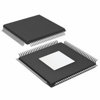
Package / Case
100-TQFP Exposed Pad, 100-eTQFP, 100-HTQFP, 100-VQFP
Resolution (bits)
12bit
Sampling Rate
800MSPS
Input Channel Type
Parallel
Digital Ic Case Style
QFP
No. Of Pins
100
Operating Temperature Range
-40°C To +85°C
Lead Free Status / RoHS Status
Lead free / RoHS Compliant
Settling Time
-
Lead Free Status / RoHS Status
Lead free / RoHS Compliant, Lead free / RoHS Compliant
Available stocks
Company
Part Number
Manufacturer
Quantity
Price
Company:

Part Number:
AD9785BSVZ
Manufacturer:
Analog Devices Inc
Quantity:
135
Company:
Part Number:
AD9785BSVZ
Manufacturer:
Analog Devices Inc
Quantity:
10 000
Company:
Part Number:
AD9785BSVZRL
Manufacturer:
Analog Devices Inc
Quantity:
10 000


AD9785/AD9787/AD9788
AD9785/AD9787/AD9788 EVALUATION BOARDS
The remainder of this data sheet describes the evaluation
boards for testing the AD9785, AD9787, and AD9788 devices.
OUTPUT CONFIGURATION
Each evaluation board contains an Analog Devices ADL5372
quadrature modulator. The AD9785/AD9787/AD9788 devices
and the ADL5372 provide an easy-to-interface DAC/modulator
combination that can be easily characterized on the evaluation
board.
Solderable jumpers can be configured to evaluate the single-
ended or differential outputs of the AD9785/AD9787/AD9788.
DIGITAL DATA
DIGITAL PICTURE OF EVALUATION BOARD
DATACLK
OUTPUT
INPUTS
OUTPUTS
INPUTS
SYNC
SYNC
Figure 79. Evaluation Board
AD9788
Rev. A | Page 54 of 64
REFCLK
INPUT
JP4 JP15
JP8
JP3
JP2
SPI
PORT
JP14
JP16
JP17
The factory default jumper configuration is as follows:
To evaluate the ADL5372 on the evaluation board, reverse the
jumper positions as follows:
Note that the ADL5372 also requires its own separate 5 V and
GND connection on the evaluation board.
Jumpers JP2, JP3, JP4, and JP8 are unsoldered.
Jumpers JP14, JP15, JP16, and JP17 are soldered.
Jumpers JP2, JP3, JP4, and JP8 are soldered.
Jumpers JP14, JP15, JP16, and JP17 are unsoldered.
S8
S9
S6
S5
RESET
ADL5372
+5V
GND
ADL5372
OUTPUT
ADL5372
LO INPUT
5V POWER
Related parts for AD9785BSVZ
Image
Part Number
Description
Manufacturer
Datasheet
Request
R

Part Number:
Description:
BOARD EVAL FOR AD9785
Manufacturer:
Analog Devices Inc
Datasheet:

Part Number:
Description:
Dual 16B, 1.0 GSPS TxDAC
Manufacturer:
Analog Devices Inc
Datasheet:

Part Number:
Description:
±1.7g Dual-Axis IMEMS Accelerometer Evaluation Board
Manufacturer:
Analog Devices Inc
Datasheet:
Part Number:
Description:
Inertial Sensor Evaluation System
Manufacturer:
Analog Devices Inc
Datasheet:
Part Number:
Description:
Manufacturer:
Analog Devices Inc
Datasheet:
Part Number:
Description:
Manufacturer:
Analog Devices Inc
Datasheet:
Part Number:
Description:
Manufacturer:
Analog Devices Inc
Datasheet:
Part Number:
Description:
Manufacturer:
Analog Devices Inc
Datasheet:
Part Number:
Description:
Manufacturer:
Analog Devices Inc
Datasheet:
Part Number:
Description:
Manufacturer:
Analog Devices Inc
Datasheet:
Part Number:
Description:
Manufacturer:
Analog Devices Inc
Datasheet:
Part Number:
Description:
Manufacturer:
Analog Devices Inc
Datasheet:
Part Number:
Description:
Manufacturer:
Analog Devices Inc
Datasheet: