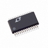
LTC1667CG Linear Technology, LTC1667CG Datasheet - Page 13

LTC1667CG
Manufacturer Part Number
LTC1667CG
Description
IC D/A CONV 14BIT 50MSPS 28-SSOP
Manufacturer
Linear Technology
Datasheet
1.LTC1668CGPBF.pdf
(24 pages)
Specifications of LTC1667CG
Settling Time
20ns
Number Of Bits
14
Data Interface
Parallel
Number Of Converters
1
Voltage Supply Source
Dual ±
Power Dissipation (max)
180mW
Operating Temperature
0°C ~ 70°C
Mounting Type
Surface Mount
Package / Case
28-SSOP
Lead Free Status / RoHS Status
Contains lead / RoHS non-compliant
Available stocks
Company
Part Number
Manufacturer
Quantity
Price
Company:
Part Number:
LTC1667CG#PBF
Manufacturer:
Linear Technology
Quantity:
135
Company:
Part Number:
LTC1667CG#PBF
Manufacturer:
LTC
Quantity:
309
APPLICATIO S I FOR ATIO
LADCOM
The LADCOM pin is the common connection for the
internal DAC attenuator ladder. It usually is tied to analog
ground, but more generally it should connect to the same
potential as the load resistors on I
LADCOM pin carries a constant current to V
mately 0.32 • (I
I
OUT A
LTC1666/LTC1667/LTC1668
0.1 F
0.1 F
and I
C1
Figure 3. Equivalent Analog Output Circuit
OUT B
0.1 F
R
C2
SET
2k
OUTFS
through the R
CLOCK SOURCE
U
LOW JITTER
REFOUT
I
COMP1
COMP2
REFIN
V
– 5V
), plus any current that flows from
SS
R
IOUT B
U
1.1k
CLK
IN
5pF
0.1 F
IOUT A
REFERENCE
PULSE GENERATOR
HP8110A DUAL
2.5V
R
1.1k
–
+
AGND DGND
IOUT A
W
OUT A
and R
Figure 4. AC Characterization Setup (LTC1668)
OUT 1 OUT 2
LADCOM
I
I
5pF
OUT A
OUT B
V
and I
IOUT B
SS
SS
V
5V
CLK
18
20
19
23
DD
of approxi-
U
1666/7/8
OUT B
resistors.
52.3
F04
DB15
52.3
0.1 F
HIGH SPEED
– 5V
. The
16-BIT
CLK
IN
DAC
LOGIC ANALYZER WITH
DB0
DIGITAL
DATA
PATTERN GENERATOR
16
Output Compliance
The specified output compliance voltage range is 1V. The
DC linearity specifications, INL and DNL, are trimmed and
guaranteed on I
I-to-V converter, but are typically very good over the full
output compliance range. Above 1V the output current will
start to increase as the DAC current steering switch
impedance decreases, degrading both DC and AC linear-
ity. Below –1V, the DAC switches will start to approach the
transition from saturation to linear region. This will de-
grade AC performance first, due to nonlinear capacitance
and increased glitch impulse. AC distortion performance
is optimal at amplitudes less than 0.5V
I
effects. At first glance, it may seem counter-intuitive to
decrease the signal amplitude when trying to optimize
SFDR. However, the error sources that affect AC perfor-
mance generally behave as additive currents, so decreas-
ing the load impedance to reduce signal voltage amplitude
will reduce most spurious signals by the same amount.
HP1663EA
OUT B
LTC1668
LADCOM
I
I
OUT A
OUT B
LTC1666/LTC1667/LTC1668
due to nonlinear capacitance and other large-signal
1666/7/8 F05
50
OUT A
50
into the virtual ground of an
110
MINI-CIRCUITS
T1–1T
P-P
on I
TO HP3589A
SPECTRUM
ANALYZER
50 INPUT
OUT A
13
and


