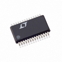
LTC1667CG Linear Technology, LTC1667CG Datasheet - Page 7

LTC1667CG
Manufacturer Part Number
LTC1667CG
Description
IC D/A CONV 14BIT 50MSPS 28-SSOP
Manufacturer
Linear Technology
Datasheet
1.LTC1668CGPBF.pdf
(24 pages)
Specifications of LTC1667CG
Settling Time
20ns
Number Of Bits
14
Data Interface
Parallel
Number Of Converters
1
Voltage Supply Source
Dual ±
Power Dissipation (max)
180mW
Operating Temperature
0°C ~ 70°C
Mounting Type
Surface Mount
Package / Case
28-SSOP
Lead Free Status / RoHS Status
Contains lead / RoHS non-compliant
Available stocks
Company
Part Number
Manufacturer
Quantity
Price
Company:
Part Number:
LTC1667CG#PBF
Manufacturer:
Linear Technology
Quantity:
135
Company:
Part Number:
LTC1667CG#PBF
Manufacturer:
LTC
Quantity:
309
PI FU CTIO S
LTC1666
REFOUT (Pin 15): Internal Reference Voltage Output.
Nominal value is 2.5V. Requires a 0.1 F bypass capacitor
to AGND.
I
1.25mA for I
AGND (Pin 17): Analog Ground.
LADCOM (Pin 18): Attenuator Ladder Common. Normally
tied to GND.
I
scale output current occurs when all data bits are 0s.
I
current occurs when all data bits are 1s.
TYPICAL PERFOR A CE CHARACTERISTICS
REFIN
OUT B
OUT A
U
(Pin 19): Complementary DAC Output Current. Full-
(Pin 16): Reference Input Current. Nominal value is
(Pin 20): DAC Output Current. Full-scale output
U
FS
= 10mA. I
U
FS
W
= I
REFIN
U
• 8.
–0.5
–2.0
–1.0
–1.5
2.0
1.5
1.0
0.5
0
0
Differential Nonlinearity
16384
DIGITAL INPUT CODE
32768
COMP1 (Pin 21): Current Source Control Amplifier Com-
pensation. Bypass to V
COMP2 (Pin 22): Internal Bypass Point. Bypass to V
with 0.1 F.
V
– 5V.
DGND (Pin 24): Digital Ground.
V
CLK (Pin 26): Clock Input. Data is latched and the output
is updated on positive edge of clock.
DB11 to DB0 (Pins 27, 28, 1 to 10 ): Digital Input Data Bits.
SS
DD
49152
(Pin 25): Positive Supply Voltage. Nominal value is 5V.
(Pin 23): Negative Supply Voltage. Nominal value is
LTC1666/LTC1667/LTC1668
1666/7/8 G19
65535
(LTC1668)
SS
with 0.1 F.
7
SS


