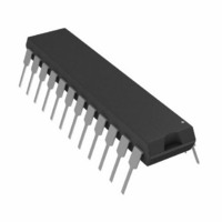
AD7538JN Analog Devices Inc, AD7538JN Datasheet - Page 10

AD7538JN
Manufacturer Part Number
AD7538JN
Description
IC DAC 14BIT W/BUFF 24-DIP
Manufacturer
Analog Devices Inc
Datasheet
1.AD7538JRZ-REEL.pdf
(16 pages)
Specifications of AD7538JN
Mounting Type
Through Hole
Rohs Status
RoHS non-compliant
Settling Time
1.5µs
Number Of Bits
14
Data Interface
Parallel
Number Of Converters
1
Voltage Supply Source
Single Supply
Power Dissipation (max)
1W
Operating Temperature
0°C ~ 70°C
Package / Case
24-DIP (0.300", 7.62mm)
Digital Ic Case Style
DIP
No. Of Pins
24
Operating Temperature Range
0°C To +70°C
Peak Reflow Compatible (260 C)
No
No. Of Bits
14 Bit
Leaded Process Compatible
No
Lead Free Status / RoHS Status
Contains lead / RoHS non-compliant
Available stocks
Company
Part Number
Manufacturer
Quantity
Price
Company:
Part Number:
AD7538JNZ
Manufacturer:
AD
Quantity:
1 145
AD7538
CIRCUIT INFORMATION
EQUIVALENT CIRCUIT ANALYSIS
Figure 5 shows an equivalent circuit for the analog section
of the AD7538 DAC. The current source I
of surface and junction leakages. The R
equivalent output resistance of the DAC, which varies with
input code. C
switches and varies from about 90 pF to 180 pF (typical values)
depending upon the digital input. g(V
equivalent voltage generator due to the reference input voltage,
V
DIGITAL SECTION
The digital inputs are designed to be both TTL and 5 V CMOS
compatible. All logic inputs are static protected MOS gates with
typical input currents of less than 1 nA. To minimize power supply
currents, it is recommended that the digital input voltages be
driven as close as possible to 0 V and 5 V logic levels.
UNIPOLAR BINARY OPERATION (2-QUADRANT
MULTIPLICATION)
Figure 6 shows the circuit diagram for unipolar binary
operation. With an ac input, the circuit performs 2-quadrant
multiplication. The code table for Figure 6 is given in Table 6.
Capacitor C1 provides phase compensation and helps prevent
overshoot and ringing when high-speed op amps are used.
REF
, and the transfer function of the DAC ladder, N.
g (V
Figure 5. AD7538 Equivalent Analog Output Circuit
OUT
REF
, N)
is the capacitance due to the current steering
R
O
I
LEAKAGE
REF
O
R/4
C
, N) is the Thevenin
resistor denotes the
OUT
LEAKAGE
R
I
AGND
OUT
FB
is composed
Rev. B | Page 10 of 16
Table 6. Unipolar Binary Code Table
Binary Number In
DAC Register
MSB
11 1111 1111 1111
10 0000 0000 0000
00 0000 0000 0001
00 0000 0000 0000
For zero offset adjustment, the DAC register is loaded with
all 0s and amplifier offset (V
Adjusting V
but it is recommended that V
(V
Hints section).
Full-scale trimming is accomplished by loading the DAC
register with all 1s and adjusting R1 so that V
(16,383/16,384). For high temperature operation, resistors
and potentiometers should have a low temperature coefficient.
In many applications, because of the excellent gain TC and
gain error specifications of the AD7538, gain error trimming is
not necessary. In fixed reference applications, full scale can also
be adjusted by omitting R1 and R2 and trimming the reference
voltage magnitude.
LDAC
V
REF
IN
WR
CS
) to maintain specified DAC accuracy (see the Application
20
21
22
DB13 TO DB0 DGND
INPUT DATA
LDAC
WR
OUT
CS
20Ω
R1
V
6
REF
1
to 0 V is not necessary in many applications,
LSB
Figure 6. Unipolar Binary Operation
19
AD7538
DIGITAL
GND
V
V
23
DD
DD
5
OS
OS
R
V
) adjusted so that V
24
2
FB
SS
be no greater than (25 × 10
Analog Output, V
−V
−V
−V
0 V
AGND
IN
IN
IN
1kΩ
I
R3
(16,383/16,384)
(8192/16,384) = −½V
(1/16,384)
OUT
10Ω
R2
4.7µF
47kΩ
C2
3
4
R4
+
OUTA
C1
33pF
ANALOG
A1
–15V
OUT
= −V
GND
OUT
AD711
is 0 V.
IN
IN
V
−6
O
)


