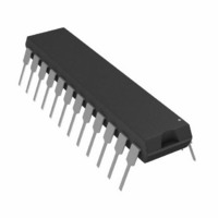
AD7538JN Analog Devices Inc, AD7538JN Datasheet - Page 11

AD7538JN
Manufacturer Part Number
AD7538JN
Description
IC DAC 14BIT W/BUFF 24-DIP
Manufacturer
Analog Devices Inc
Datasheet
1.AD7538JRZ-REEL.pdf
(16 pages)
Specifications of AD7538JN
Mounting Type
Through Hole
Rohs Status
RoHS non-compliant
Settling Time
1.5µs
Number Of Bits
14
Data Interface
Parallel
Number Of Converters
1
Voltage Supply Source
Single Supply
Power Dissipation (max)
1W
Operating Temperature
0°C ~ 70°C
Package / Case
24-DIP (0.300", 7.62mm)
Digital Ic Case Style
DIP
No. Of Pins
24
Operating Temperature Range
0°C To +70°C
Peak Reflow Compatible (260 C)
No
No. Of Bits
14 Bit
Leaded Process Compatible
No
Lead Free Status / RoHS Status
Contains lead / RoHS non-compliant
Available stocks
Company
Part Number
Manufacturer
Quantity
Price
Company:
Part Number:
AD7538JNZ
Manufacturer:
AD
Quantity:
1 145
BIPOLAR OPERATION (4-QUADRANT
MULTIPLICATION)
The recommended circuit diagram for bipolar operation is
shown in Figure 8. Offset binary coding is used. The code table
for Figure 8 is given in Table 7.
With the DAC loaded to 10 0000 0000 0000, adjust R1 for V
0 V. Alternatively, one can omit R1 and R2 and adjust the ratio
of R5 and R6 for V
plished by adjusting the amplitude of V
value of R7.
The values given for R1, R2 are the minimum necessary to
calibrate the system for Resistors R5, R6, R7 ratio matched to
0.1%. System linearity error is independent of resistor ratio
matching and is affected by DAC linearity error only.
When operating over a wide temperature range, it is important
that the resistors be of the same type so that their temperature
coefficients match.
LOW LEAKAGE CONFIGURATION
For CMOS multiplying DAC, as the device is operated at higher
temperatures, the output leakage current increases. For a 14-bit
resolution system, this can be a significant source of error. The
AD7538 features a leakage reduction configuration (U.S. Patent
No. 4,590,456) to keep the leakage current low over an extended
temperature range. One may operate the device with or without
this configuration. If V
exhibits normal output leakage currents at high temperatures.
To use the low leakage facility, V
of approximately −0.3 V as in Figure 6 and Figure 8. A simple
resistor divider (R3, R4) produces approximately −300 mV
from −15 V. The C2 capacitor in parallel with R3 is an integral
part of the low leakage configuration and must be 4.7 μF or
greater. Figure 7 is a plot of leakage current vs. temperature
for both conditions. It clearly shows the improvement gained
by using the low leakage configuration.
O
= 0 V. Full-scale trimming can be accom-
SS
(Pin 24) is tied to AGND then the DAC
LDAC
V
IN
WR
CS
SS
should be tied to a voltage
20
21
22
50Ω
DB13 TO DB0 DGND
IN
INPUT DATA
R1
LDAC
WR
CS
V
or by varying the
6
REF
1
19
AD7538
DIGITAL
GND
V
V
23
DD
DD
5
R
V
Figure 8. Bipolar Operation
24
2
FB
SS
O
Rev. B | Page 11 of 16
=
AGND
1kΩ
I
R3
OUT
22Ω
R2
4.7µF
47kΩ
C2
3
4
R4
+
Table 7. Bipolar Code Table for the Offset Binary Circuit
of Figure 8
Binary Number In
DAC Register
MSB
11 1111 1111 1111
10 0000 0000 0001
10 0000 0000 0000
01 1111 1111 1111
00 0000 0000 0000
C1
33pF
ANALOG
GND
Figure 7. Graph of Typical Leakage Current vs. Temperature for AD7538
A1
–15V
AD711
60
50
40
30
20
10
5kΩ, 10%
0
R8
10kΩ
R5
30
R6
20kΩ
LSB
40
V
V
DD
REF
20kΩ
A2
R7
50
= 15V
AD711
= 10V
TEMPERATURE (°C)
60
70
V
0 V
Analog Output V
+V
+V
−V
−V
O
80
IN
IN
IN
IN
(8191/8192)
(1/8192)
(1/8192)
(8191/8192)
90
V
100 110 120
SS
= 0V
V
SS
OUT
= –0.3V
AD7538


