AD660SQ Analog Devices Inc, AD660SQ Datasheet - Page 10
AD660SQ
Manufacturer Part Number
AD660SQ
Description
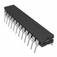
IC DAC 16BIT MONO W/VREF 24-CDIP
Manufacturer
Analog Devices Inc
Series
DACPORT®r
Datasheet
1.AD660ARZ.pdf
(20 pages)
Specifications of AD660SQ
Rohs Status
RoHS non-compliant
Settling Time
6µs
Number Of Bits
16
Data Interface
Serial
Number Of Converters
1
Voltage Supply Source
Analog and Digital, Dual ±
Power Dissipation (max)
625mW
Operating Temperature
-55°C ~ 125°C
Mounting Type
Through Hole
Package / Case
24-CDIP (0.300", 7.62mm)
Available stocks
Company
Part Number
Manufacturer
Quantity
Price


AD660
THEORY OF OPERATION
The AD660 uses an array of bipolar current sources with MOS
current steering switches to develop a current proportional to the
applied digital word, ranging from 0 mA to 2 mA. A segmented
architecture is used, where the most significant four data bits
are thermometer decoded to drive 15 equal current sources.
The lesser bits are scaled using a R-2R ladder, then applied
together with the segmented sources to the summing node of
the output amplifier. The internal span/bipolar offset resistor
can be connected to the DAC output to provide a 0 V to 10 V
span, or it can be connected to the reference input to provide a
−10 V to +10 V span.
ANALOG CIRCUIT CONNECTIONS
Internal scaling resistors provided in the AD660 can be connected
to produce a unipolar output range of 0 V to 10 V or a bipolar
output range of −10 V to +10 V. Gain and offset drift are mini-
mized in the AD660 because of the thermal tracking of the
scaling resistors with other device components.
UNIPOLAR CONFIGURATION
The configuration shown in Figure 8 provides a unipolar 0 V to
10 V output range. In this mode, 50 Ω resistors are tied between
the SPAN/BIPOLAR OFFSET terminal (Pin 22) and V
and between REF OUT (Pin 24) and REF IN (Pin 23). It is possible
to use the AD660 without any external components by tying Pin 24
directly to Pin 23 and Pin 22 directly to Pin 21. Eliminating
these resistors increases the gain error by 0.25% of FSR.
REF IN
LDAC
HBE
SER
CLR
CLEAR SELECT
16
17
18
19
23
LBE/
15
CONTROL
LOGIC
10kΩ
REF OUT
10V REF
24
CS
Figure 7. Functional Block Diagram
14
DB0/
DB8/
SIN
12
–V
16-BIT LATCH
16-BIT LATCH
1
EE
DB1/DB9/
16-BIT DAC
DATADIR
11
+V
2
CC
DB15
DB7/
5
+V
10.05kΩ
AD660
3
LL
10kΩ
DGND
4
OUT
13
22
21
20
S
SPAN/
BIPOLAR
OFFSET
V
AGND
(Pin 21),
OUT
OUT
Rev. B | Page 10 of 20
If it is desired to adjust the gain and offset errors to zero, this
can be accomplished using the circuit shown in Figure 9. The
adjustment procedure is as follows:
1.
2.
REF IN
LDAC
REF IN
HBE
SER
CLR
LDAC
CLEAR SELECT
HBE
SER
CLR
Figure 9. 0 V to 10 V Unipolar Voltage Output with Gain and Offset
Zero adjust.
Turn all bits off and adjust the zero trimmer, R4, until the
output reads 0.000000 V (1 LSB = 153 μV).
Gain adjust.
Turn all bits on and adjust the gain trimmer, R1, until the
output is 9.999847 V. (Full scale is adjusted to 1 LSB less
than the nominal full scale of 10.000000 V.)
CLEAR SELECT
100Ω
R1
16
17
18
19
23
LBE/
16
17
18
19
23
REF OUT
50Ω
15
R1
LBE/
CONTROL
15
REF OUT
LOGIC
10kΩ
CONTROL
Figure 8. 0 V to 10 V Unipolar Voltage Output
10V REF
LOGIC
10kΩ
10V REF
24
CS
14
24
CS
14
DB0/
DB8/
SIN
12
–V
DB0/
DB8/
16-BIT LATCH
16-BIT LATCH
SIN
1
12
EE
DB1/DB9/
16-BIT DAC
DATADIR
–V
16-BIT LATCH
16-BIT LATCH
1
EE
16-BIT DAC
DB1/DB9/
11
DATADIR
Adjustment
11
+V
2
CC
DB15
DB7/
+V
5
2
CC
DB15
DB7/
5
AD660
+V
10kΩ
3
10.05kΩ
LL
+V
AD660
3
LL
BIPOLAR
DGND
10.05kΩ
OFFSET
10kΩ
SPAN/
DGND
S
OUT
4
S
OUT
4
13
22
21
20
V
50Ω
OUT
AGND
13
22
21
20
R2
OUTPUT
V
SPAN/
BIPOLAR
OFFSET
AGND
50Ω
OUT
R2
16k
OUTPUT
R3
+V
–V
EE
CC
10k
R4
Related parts for AD660SQ
Image
Part Number
Description
Manufacturer
Datasheet
Request
R

Part Number:
Description:
±1.7g Dual-Axis IMEMS Accelerometer Evaluation Board
Manufacturer:
Analog Devices Inc
Datasheet:

Part Number:
Description:
Inertial Sensor Evaluation System
Manufacturer:
Analog Devices Inc
Datasheet:
Part Number:
Description:
Manufacturer:
Analog Devices Inc
Datasheet:
Part Number:
Description:
Manufacturer:
Analog Devices Inc
Datasheet:
Part Number:
Description:
Manufacturer:
Analog Devices Inc
Datasheet:
Part Number:
Description:
Manufacturer:
Analog Devices Inc
Datasheet:
Part Number:
Description:
Manufacturer:
Analog Devices Inc
Datasheet:
Part Number:
Description:
Manufacturer:
Analog Devices Inc
Datasheet:
Part Number:
Description:
Manufacturer:
Analog Devices Inc
Datasheet:
Part Number:
Description:
Manufacturer:
Analog Devices Inc
Datasheet:
Part Number:
Description:
Manufacturer:
Analog Devices Inc
Datasheet:
Part Number:
Description:
Manufacturer:
Analog Devices Inc
Datasheet:
Part Number:
Description:
Manufacturer:
Analog Devices Inc
Datasheet: