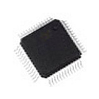
PSD813F2VA-15MI STMicroelectronics, PSD813F2VA-15MI Datasheet - Page 32

PSD813F2VA-15MI
Manufacturer Part Number
PSD813F2VA-15MI
Description
Manufacturer
STMicroelectronics
Datasheet
1.PSD813F2VA-15MI.pdf
(109 pages)
Specifications of PSD813F2VA-15MI
Operating Temperature (max)
85C
Operating Temperature (min)
-40C
Operating Temperature Classification
Industrial
Package Type
PQFP
Mounting
Surface Mount
Pin Count
52
Lead Free Status / Rohs Status
Compliant
Available stocks
Company
Part Number
Manufacturer
Quantity
Price
- Current page: 32 of 109
- Download datasheet (909Kb)
PSD813F2V, PSD854F2V
PAGE REGISTER
The 8-bit Page Register increases the addressing
capability of the MCU by a factor of up to 256. The
contents of the register can also be read by the
MCU. The outputs of the Page Register (PGR0-
PGR7) are inputs to the DPLD decoder and can be
included
CSBOOT0-CSBOOT3), and SRAM Select (RS0)
equations.
Figure 12. Page Register
32/109
in
the
Sector
Select
RESET
R / W
D0 - D 7
(FS0-FS7,
D 0
D 1
D 2
D 3
D 4
D 5
D 6
D 7
Doc ID 10552 Rev 3
REGISTER
PAGE
Q 0
Q 1
Q 2
Q 3
Q 4
Q 5
Q 6
Q 7
PGR0
PGR1
PGR2
PGR3
PGR4
PGR5
PGR6
PGR7
If memory paging is not needed, or if not all 8 page
register bits are needed for memory paging, then
these bits may be used in the CPLD for general
logic. See Application Note AN1154.
Figure
flops in the register are connected to the internal
data bus D0-D7. The MCU can write to or read
from the Page Register. The Page Register can be
accessed at address location CSIOP + E0h.
12
shows the Page Register. The eight flip-
DPLD
CPLD
PLD
AND
INTERNAL
SELECTS
AND LOGIC
AI02871B
Related parts for PSD813F2VA-15MI
Image
Part Number
Description
Manufacturer
Datasheet
Request
R

Part Number:
Description:
Manufacturer:
STMicroelectronics
Datasheet:

Part Number:
Description:
Flash In-system Programmable Isp Peripherals For8-bits Mcus, 3v
Manufacturer:
STMicroelectronics
Datasheet:

Part Number:
Description:
Manufacturer:
STMicroelectronics
Datasheet:

Part Number:
Description:
Flash In-System-Programmable Microcontroller Peripheral
Manufacturer:
STMicroelectronics

Part Number:
Description:
Manufacturer:
STMicroelectronics
Datasheet:

Part Number:
Description:
STMicroelectronics [RIPPLE-CARRY BINARY COUNTER/DIVIDERS]
Manufacturer:
STMicroelectronics
Datasheet:

Part Number:
Description:
STMicroelectronics [LIQUID-CRYSTAL DISPLAY DRIVERS]
Manufacturer:
STMicroelectronics
Datasheet:

Part Number:
Description:
BOARD EVAL FOR MEMS SENSORS
Manufacturer:
STMicroelectronics
Datasheet:

Part Number:
Description:
NPN TRANSISTOR POWER MODULE
Manufacturer:
STMicroelectronics
Datasheet:

Part Number:
Description:
TURBOSWITCH ULTRA-FAST HIGH VOLTAGE DIODE
Manufacturer:
STMicroelectronics
Datasheet:

Part Number:
Description:
Manufacturer:
STMicroelectronics
Datasheet:


